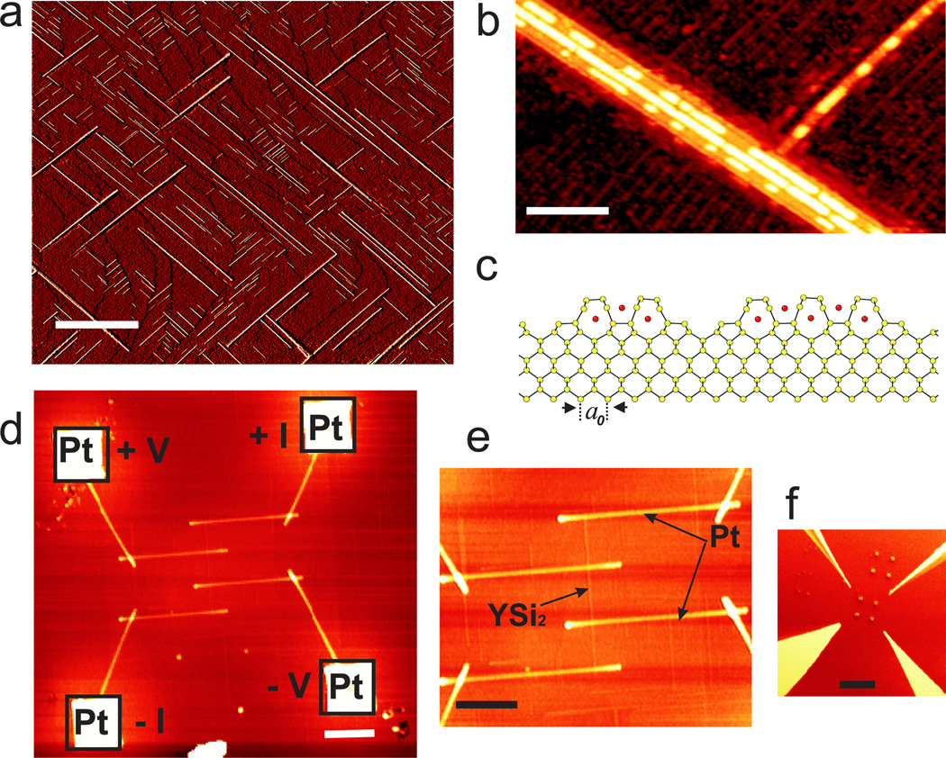
Figure 1.
Scanning probe characterization of YSi2 nanowires. (a) STM image showing numerous YSi2 wire bundles on the Si(100) surface before patterning (scale bar: 450 nm). The tunneling parameters are −1.9 V and 0.08 nA. (b) Enlarged area of panel (a) showing two orthogonal bundles with segments of a second silicide layer (scale bar: 22 nm). (c) Cross-sectional structure of a wire bundle containing a 3a0 and a 5a0 nanowire, according to Ref. 12, with a0 = 0.384 nm; silicon atoms are shown in yellow and yttrium atoms are shown in red. (d) Non-contact atomic force microscopy (AFM) image of a capped YSi2 nanowire contacted by Pt leads and Pt contact pads (squares) (scale bar: 400 nm). (e) AFM image of the center area of the device presented in (d), showing the Pt leads and a YSi2 nanowire bridging the leads (scale bar: 300 nm). (f) Scanning electron microscopy (SEM) image showing four STM tips in close proximity to the Pt pads (scale bar: 5 µm).

