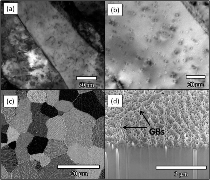
Figure 5. He+ ion irradiated tungsten samples.
TEM and SEM micrographs of ultrafine-grained tungsten taken at room temperature after being irradiated with 2 keV He+ to a fluence of 3.2 × 10¹⁹ ions.m−2 at 950°C: (a) adjacent ultrafine grains with high concentrations of point defect clusters and dislocations; and (b) an ultrafine tungsten grain with a uniform areal bubble density. The diffraction contrast around the bubbles suggests they are combined with dislocation loops and/or are over pressurized as both these phenomena could induce a strain field. Panel (c) shows a secondary electron image formed using a Ga+ ion beam of an ultrafine-grained sample irradiated with 30 eV He+ ions at 1200°C to a fluence of 1026 ions.m−2 in a complementary experiment; and (d) shows a cross-sectional secondary electron image of the sample in (c) showing nanostructured grains decorated with surface pores and a bowed grain boundary.

