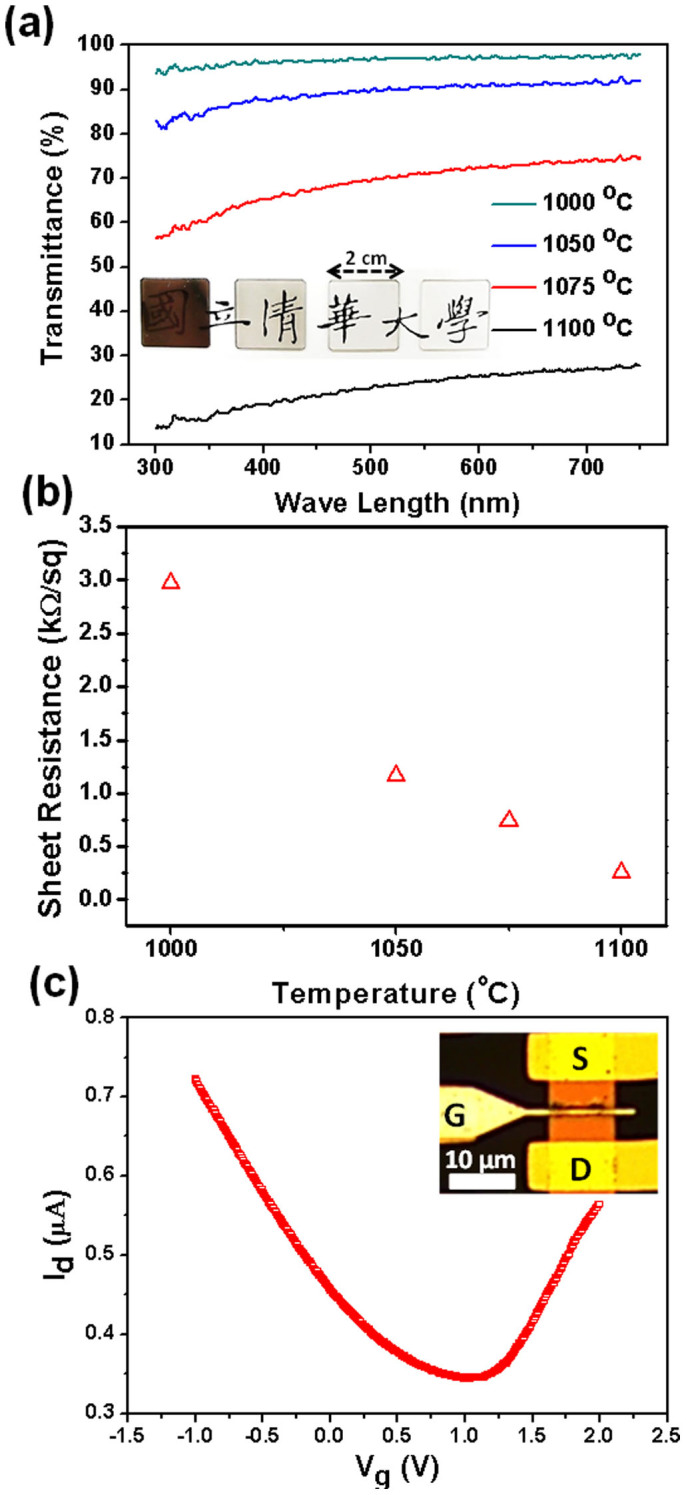
Figure 6.

(a) Optical transmittance measurements from 300 to 750 nm for the graphene at different deposition temperatures. Inset shows optical images of the graphene deposited on quartz substrate at temperatures from 1000, 1050, 1075, and 1100°C for 5 minutes at 60 torr, respectively. (b) The corresponding sheet resistance in (a). (c) shows field effect transistor behaviors, with which single graphene grown at 1100°C for 5 minutes at 60 torr was used as a channel material. Inset shows the optical image, for which the channel length (L) of ~2 μm and channel width (W) of 5 μm can be observed, respectively.
