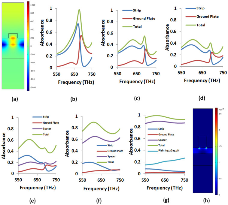
Figure 7.
(a) Hz (A/m) for a higher order plasmonic mode resonating at 672 THz (i.e., in the neighborhood of Point 3) supported by the near-perfect absorber with the parameters given in Table 1. Absorbance in different parts of the perfect absorber (b) operating in the neighborhood of Point 3 (legends not shown for clarity, same as other plots), (c) when the strip thickness in the absorber increases to ts = 40 nm, and (d) when both the strip and the ground plate have ts = tg = 60 nm thickness. All the other parameters are kept fixed and the same as in Table 1. Absorbance in different parts of the absorber achieved by the BSDT process described in (b)–(d) followed by the gradual incorporation of the true complex permittivity such that (e)  , (f)
, (f)  , and (g)
  . The total absorbance in plain In0.54Ga0.46N layer of the same thickness (i.e., d = 31 nm) is also shown for comparison. (h) Power loss density (W/m3) distribution for the near-perfect absorber in (g) for the third selected frequency of 695 THz in the In0.54Ga0.46N data (i.e., Point 3 in Table 1). Significant portion of the power (i.e., over 85%) is absorbed inside the In0.54Ga0.46N layer.

