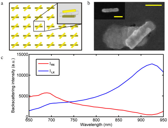
Figure 2. PCN array.
(a) Geometry of a Plasmonic chiral nanoparticle array (inset: 3D sketch of an individual L-PCN) (b) SEM image of a single L-PCN (inset: SEM image of the bottom nanorod before the dielectric layer was deposited). Scale bars: 100 nm. (c) FDTD simulated backscattering (depolarization component) intensities for LCP (blue) and RCP (red) incident beams, respectively, from the L-PCN.

