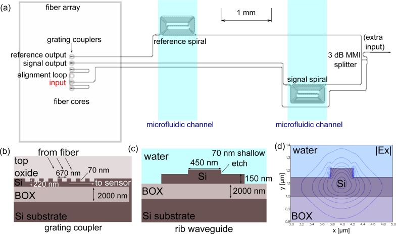
Fig. 2.
(a) SOI chip design with indication of the microfluidic channels (b) design of the grating coupler and (c) rib waveguide design that is used in the sensor circuit. (d) contour plot of the amplitude of the dominant Ex field of the fundamental TE-mode of a 450 nm wide rib waveguide that is used for evanescent sensing.

