Figure 4.

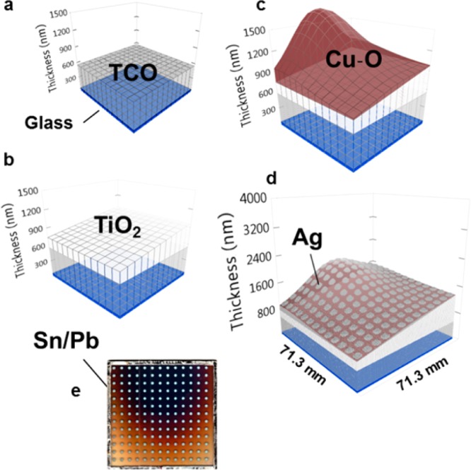
Fabrication of PV combinatorial device library (note that the thickness scale is adjusted to amplify the differences and represents real values as explained below): (a) TCO-coated glass (b) sprayed with a gradual compact TiO2 layer, followed by (c) pulsed laser deposition (PLD) of Cu–O with a characteristic shape originating from the laser plume. (d) Round Ag back contacts sputtered on top of the Cu–O layer with a 13 × 13 mask template, forming a grid of 169 distinct devices. Subsequently (e) a square common front contact is soldered ultrasonically from Sn/Pb directly onto the TCO.
