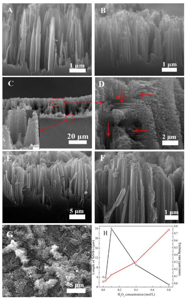
Figure 3.
SEM images of etched lightly doped silicon wafer under various concentration of H2O2. (A) 0, (B) 0.03, (C,D) 0.1, (E,F) 0.4, and (G) 0.8 mol/L. (H) The lengths of SiNWs and etching rates as function of H2O2 concentration. The inset in (C) shows the magnified image of SiNWs, the part in the dotted box is magnified in (D) and the pore channels are marked as red arrows.

