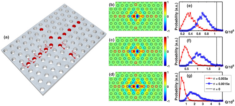
Figure 3.
(a): The design of the H0 cavity. For quality factor optimization, shifts of the positions of the five neighboring holes in the x-direction and the two neighboring holes in the y-direction were introduced, labeled as S1x, S2x, S3x, S4x, S5x, S1y and S2y in the Figure. (b)–(d): Electric field (Ey) profiles of three optimized designs with increasing Q and V. (b): S1x = 0.216a, S2x = 0.103a, S3x = 0.123a, S4x = 0.004a, S5x = 0.194a, S1y = −0.017a, S2y = 0.067a. (c): S1x = 0.280a, S2x = 0.193a, S3x = 0.194a, S4x = 0.162a, S5x = 0.113a, S1y = −0.016a, S2y = 0.134a. (d): S1x = 0.385a, S2x = 0.342a, S3x = 0.301a, S4x = 0.229a, S5x = 0.116a, S1y = −0.033a, S2y = 0.093a. (e): Histograms showing the probability of occurrence of different Qe-values in the design of panel (b), for two different disorder magnitudes: σ = 0.003a (red) and σ = 0.0015a (blue). The black line indicates the value of Qt. (f)–(g): Same as (e), for the designs of (c)–(d). The σ = 0 line in panel (g) is not visible as Qt occurs beyond the axis boundary.

