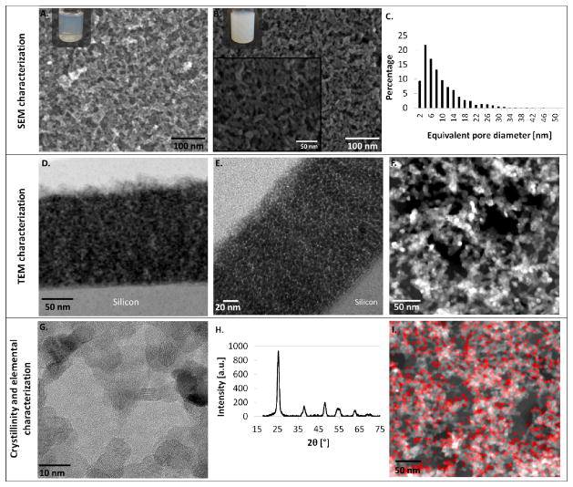
Figure 2.
Titanium dioxide nanoporous structures. A and B. Top surface SEM images of the phage film coated with titania and annealed at 450°C. In A, the reaction was stopped early (after 40 minutes) and in B the coating was allowed to proceed fully for an optimal reaction time of an hour. The color of the titania solution at each time point is show in the respective inset. Images of films coated with TiO2 for an hour are shown at two different magnifications. C. Pore size distribution based on 5 different top surface SEM images. The mean pore diameter is 8.1 nm, with a standard deviation of 6.5 nm for an hour reaction in TiCl4. D and E. TEM images of the cross-section of a titania network formed after reacting in TiCl4 for one hour reaction. The film was constructed on silicon and cross-sectioned with a focused ion beam, (D – STEM-Bright Field (BF) image, E – TEM image). F. STEM-HAADF (high angle annular dark field) image contrasting the titania nanowire mesh (brighter), from the silicon nitride support film that the phage film was constructed on (pale grey), and empty spaces (black). G and H. Crystallinity of titania-coated phage films after annealing at 450°C (G – TEM image showing lattice fringes of crystalline titania nanoparticles, H – X-Ray diffraction spectrum of resulting anatase titania). I. STEM-Bright Field image and elemental mapping of titanium for a titania nanowire mesh constructed on a silicon nitride support film.

