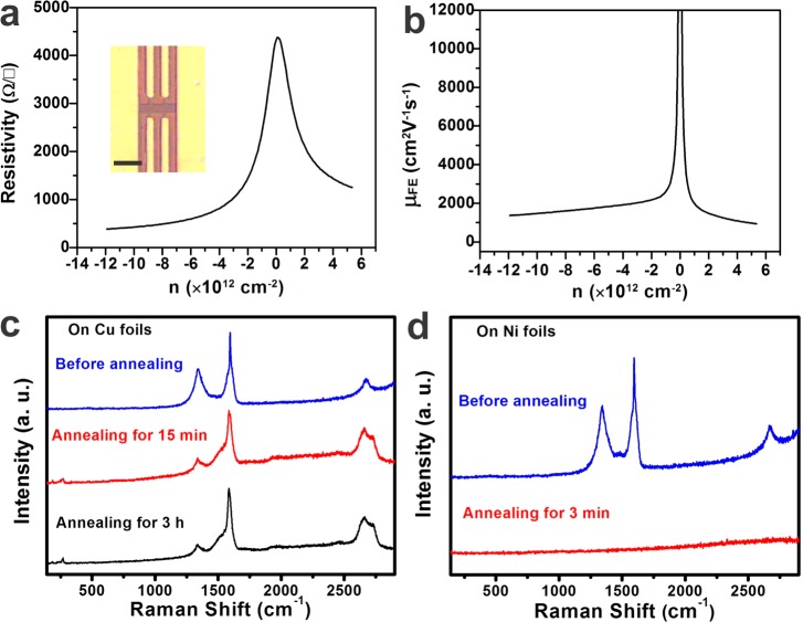
Figure 4.
Electrical properties and control growth experiments of rebar graphene on Cu- and Ni-foils. (a) Resistivity as a function of carrier density measured at room temperature. The inset is an optical image of the fabricated rebar graphene Hall bar field effect transistor on a SiO2/Si substrate; the scale bar is 20 μm. (b) Plot of density-dependent field effect mobility of rebar graphene vs carrier density from the device indicated in the inset of panel a. (c) Raman spectra indicating the weak etching ability of Cu on SWCNTs at 1080 °C for 15 min and 3 h. (d) Raman spectra demonstrating the high etching ability of Ni on SWCNTs. Here, DF-SWCNTs were used as raw materials and deposited on surfaces of Cu- and Ni-foils using a spin-coater (see the Supporting Information for details).

