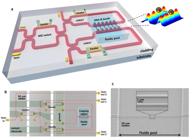
Figure 1. Design and fabrication of nanophotonic standing-wave array traps (nSWAT) device.
a, A schematic illustration of the device design. nSWATs were implemented with silicon waveguides on a silicon-on-insulator (SOI) platform (Methods). Laser input to the waveguide is partitioned to two nSWATs using an MZI. nSWATs have a 50/50 waveguide beam splitter with connected output arms to create counter-propagating waves. There are three microheaters located above the waveguides: one in the MZI to control the partition of the laser into the two nSWATs, and two more to control the trap positions in each nSWAT. The microheaters and waveguides are buried in oxide, except for the exposed waveguides in the fluidic pool trapping region. The inset shows an array of traps with a DNA molecule suspended between two beads that are held by nSWATs. The colored 3-D plot shows the calculated energy density of standing waves on both waveguides (see also Figure S1).
b, An optical microscope image of the fabricated device (false colored). Each microheater is located on one of the two arms after a splitter while an unconnected strip of metal is located on the other arm to balance potential optical loss introduced by the metal in the proximity of a waveguide. The waveguides are made of silicon on a SOI wafer.
c, Scanning electron micrographs of the waveguides in the trapping region. The waveguides are 440 nm in width and 250 nm in height. Note that while all waveguides reside in the same plane, the protective layer of oxide outside the fluid channel gives the illusion that they do not by amplifying the structure of the underlying waveguides.

