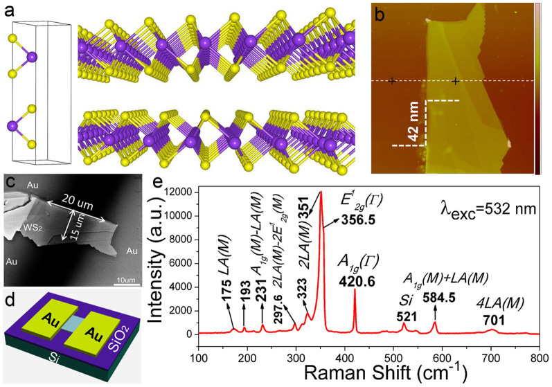
Figure 1. Characterization of the multilayer WS2 nanoflakes.
(a) Primitive cell and three-dimensional schematic representation of a typical WS2 structure with the sulfur atoms in yellow and the tungsten atoms in purple. Atomic force microscopy (AFM) image (b) and scanning electron microscopy (SEM) image (c) of the actual transistor based on multilayer WS2 nanoflakes. (d) Schematic diagram of the device. The thickness of WS2 nanoflakes is 42 nm. The width (W) and length (L) of the channel in the device is 15 μm and 20 μm, respectively. (e) Room-temperature Raman spectrum from the multilayer WS2 nanoflakes, using the 532 nm laser.

