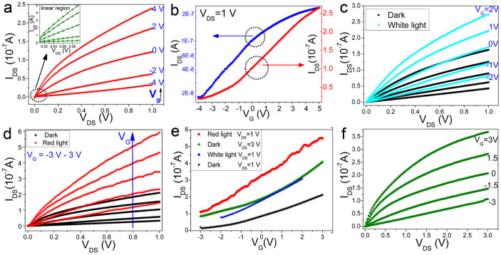
Figure 2. Field effect of the multilayer WS2 nanoflakes.
(a) Output characteristics of the transistor based on multilayer WS2 nanoflakes using Au/Au as the drain/source electrodes. The inset is linear region at low source drain voltage. (b) Transfer characteristics of the device at a fixed VDS of 1 V on a log scale (left y axis) and on a linear scale (right y axis). All measurements were performed in air at room temperature with the absence of light. Output characteristics of the device with (c) white light (15 mW/cm2) from LEDs and (d) red light (633 nm, 15 mW/cm2) from red lasers. (e) Transfer characteristics of the devices in dark and under light illumination. (f) Output characteristics of the devices in dark with VDS ranging from 0 to 3 V.

