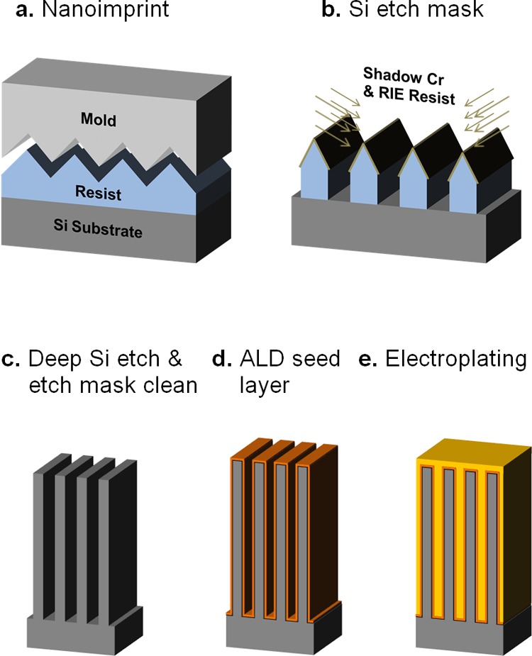
Figure 1.

Illustration of the fabrication process for 200 nm period hard X-ray phase gratings. (a) The grating lines are patterned on a polymer resist layer on the silicon wafer by nanoimprint lithography. (b) Chromium shadowing and reactive ion etching of the resist layer forms the etch mask for the silicon wafer. (c) Cryogenic deep silicon etching produces a grating mold of high aspect ratio, followed by plasma cleaning of the etch mask. (d) Atomic layer deposition of Al2O3 and Pt lays the electroplating seed layer. (e) Electroplating of gold fills the trenches of the mold.
