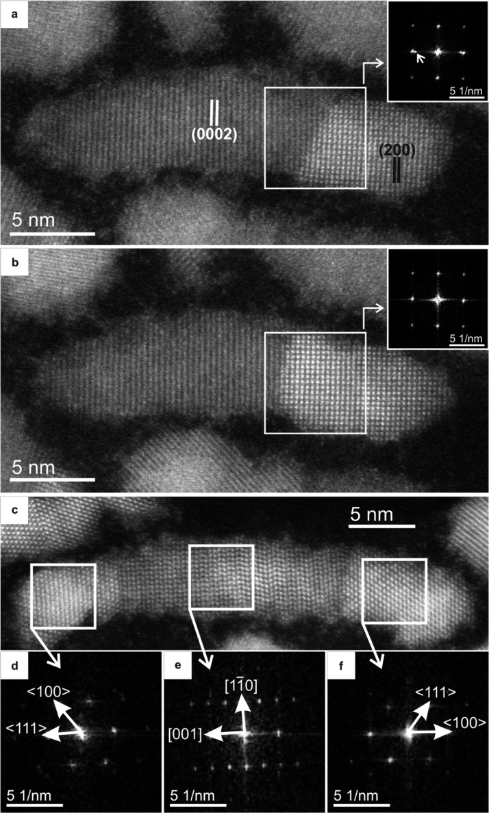
Figure 2.
Atomic-resolution HAADF-STEM images of CdSe-PbSe HNCs. PbSe has cubic rock salt (RS) crystal structure with a lattice constant20 of 6.13 Å, whereas CdSe has a hexagonal wurtzite (WZ) crystal structure with lattice parameters21a = 4.29 Å and c = 7.01 Å. The CdSe WZ (0002) spacing is 3.5 Å and PbSe RS (200) spacing is 3.1 Å. With heating from 160 °C (a) to 180 °C (b) with a heating rate of 10 degrees/min, WZ CdSe nanorods started to transform to RS PbSe. The insets are Fourier transforms (FTs) taken from the white squares in each image. The spot depicted with an arrow in the inset FT of panel a corresponds to WZ CdSe(0002) spacing. It disappeared in the inset FT of panel b, confirming the WZ to RS transformation. Supporting Information Movie S4 shows the transformation with atomic resolution. (c) HAADF-STEM image of a PbSe-CdSe dumbbell HNC. Stacking faults and a dislocation are present in the CdSe nanorod domain. The interface at the left-hand side is {111}PbSe/{0001}CdSe (panel d), whereas the interface at the right-hand side is {100}PbSe/{0001}CdSe (panel f).

