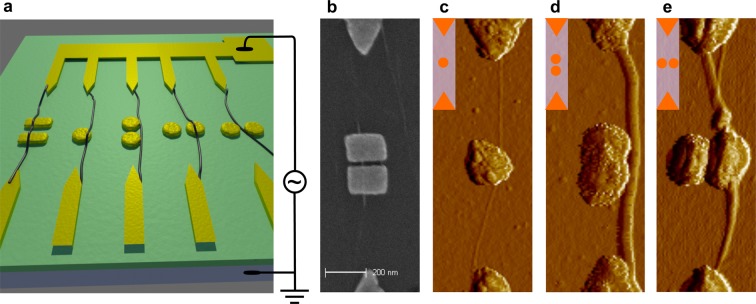
Figure 1.

(a) Schematic of plasmonic antennas placed between interconnected biased electrodes and counter electrodes (yellow, in the front) that are capacitively coupled to the p-type silicon substrate (blue) via 290 nm of SiO2 (green). Carbon nanotubes dispersed in aqueous solution assemble between the electrodes due to dielectrophoretic forces and form nanoplasmonic-nanotube systems shown in the form of SEM (b) and AFM error images (c–e). CNTs may be suspended over a cavity formed by rods (b), cross a nanodisk (c,e) or be placed next to a plasmonic structure (d).
