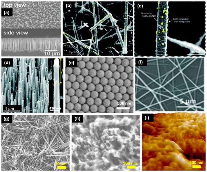
Figure 2.
Nanostructured surfaces fabricated by various processes. (a) SEM images of densely packed silicon nanopillars with diameters of 100–200 nm. These were produced using wet chemical etching by Ag+ and hydrofluoric acid. Reprinted with permission from John Wiley and Sons (Wang et al. Angew. Chem. Int. Ed. Engl. 2009; 48(47): 8970–8973). (b) SEM image of silicon nanowires (SiNWs) produced by vapor–liquid–solid method (SiNW diameter ~ 200 nm). (c) Magnified image of SiNWs bound to biotin-gold nanoparticles. Gold nanoparticles are highlighted as yellow for better presentation. Reprinted (adapted) with permission from (Kim et al. Nano Lett., 10 (8) (2010) 2877–2883). Copyright (2010) American Chemical Society. (d) SEM image of Au nanoclusters coated SiNWs produced by rapid thermal chemical vapor deposition (diameter ~100 nm). Inset shows the magnified images of Au coated SiNWs. Reprinted (adapted) with permission from (Park et al. Nano Lett. 12 (2012) 1638–1642). Copyright (2012) American Chemical Society. (e) SEM image of close-packed arrays of silica nanobeads with uniform diameter of 319 nm. The nanobeads were deposited on glass to control the substrate topography. Reprinted (adapted) with permission from (Wang et al. Langmuir 27 (2011) 11229–11237). Copyright (2011) American Chemical Society. (f) SEM image of TiO2 nanofibers with diameter ranging from 100 to 300 nm. These nanofibers were fabricated and coated on silicon wafer using electrospinning and calcination. Reprinted with permission from John Wiley and Sons (Zhang et al. Adv. Mater. 24 (20) (2012) 2756–2760). (g, h) Micro needles and nanotextured surfaces were synthesized by chemical etching of chicken eggshell with sulfuric and hydrochloric acid. Micro needles and nanotextured surfaces were made of calcium sulphate crystals and calcium carbonate, respectively. (i) AFM image of PDMS surface that was cured on nanotextured chicken eggshell. Reprinted with permission from Institute of Physics (Asghar et al. Nanotechnology 23 (2012) 475601).

