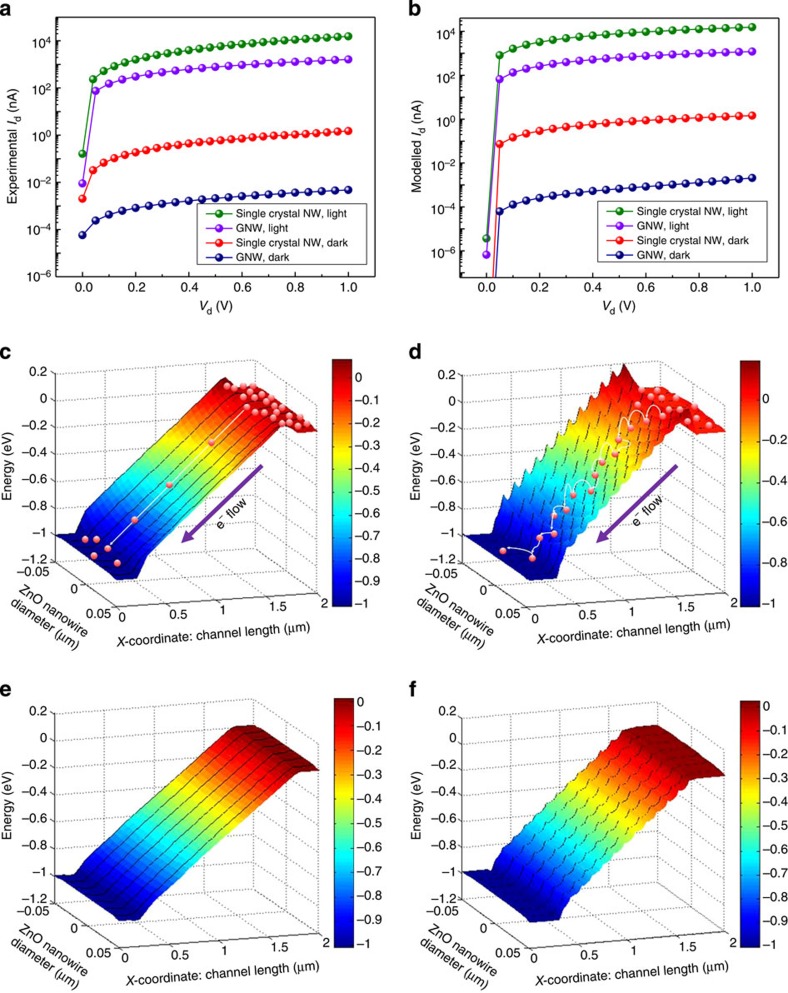
Figure 4. Device modeling of a GNW photodetector.
Comparison of the experimental (a) and modelled (b) I–V curves of photodetectors made of an individual single crystal ZnO NW and a GNW. (c) and (d) are modelled conduction band energy profiles of a single crystalline NW device and a GNW device under dark condition, respectively. And (e) and (f) are the corresponding modelled results under 100 μW cm−2 UV illumination, respectively.

