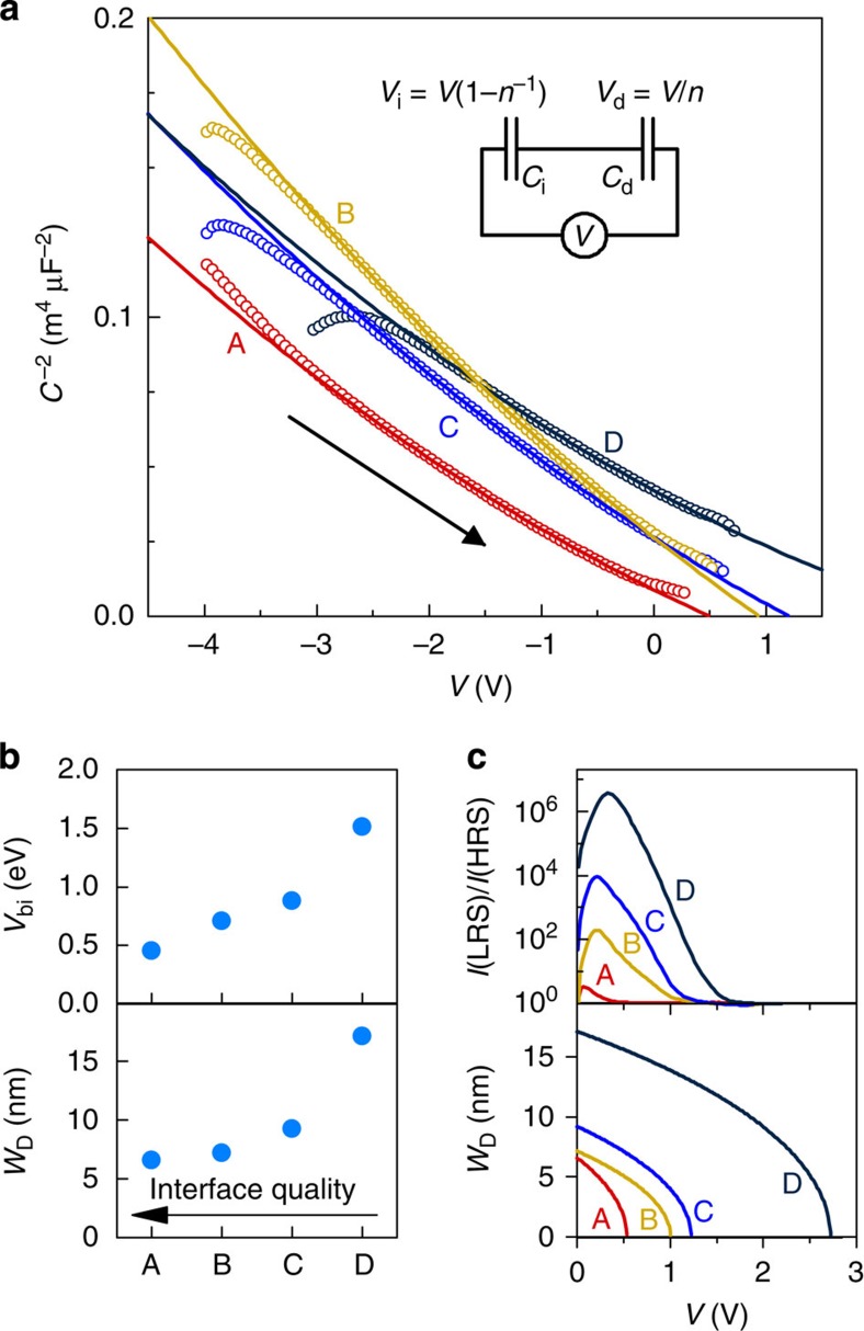
Figure 2. C–V characteristics of the devices.
(a) C–V data for all samples in the HRS, plotted as C−2 versus V. The lines are fits to Equation (6). The inset shows the equivalent circuit model and the voltage partitioning between the depletion and interface layer capacitances, Cd and Ci. (b) Extracted built-in potentials Vbi and depletion widths WD at zero bias. (c) Ratio between the currents in LRS and HRS as the function of voltage (top) and the calculated depletion width under forward bias (bottom).

