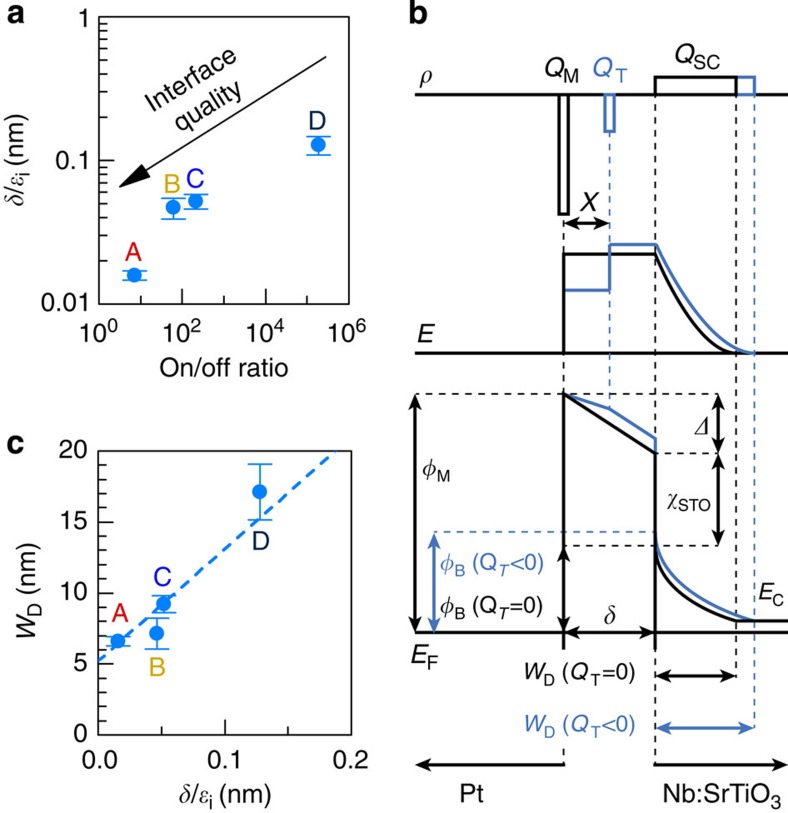
Figure 4. Influence of the interface layer on the Schottky junction parameters.
(a) Correlation between the magnitude of resistive switching and the interface layer thickness. (b) Effect of a negative trapped charge QT on a Pt/Nb:SrTiO3 junction. Top: charge density (ρ) distribution profile with and without QT. Middle: electric field (E) profile with and without QT. Bottom: band profile. The Schottky barrier is increased by a negative QT. (c) Correlation between the zero-bias depletion width and the interface layer thickness.

