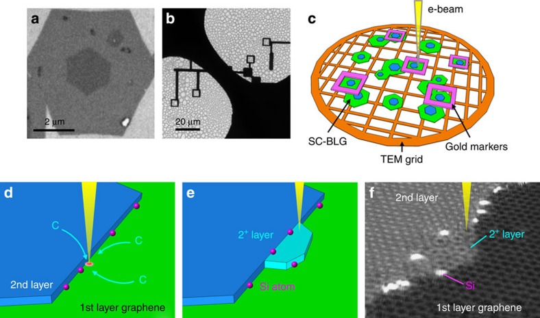
Figure 1. Scheme of graphene growth by e-beam in TEM.
(a) Scanning electron microscopy image of a SC-BLG, (b) marked by e-beam lithography, (c) transferred to a Mo TEM grid and (d) schematic drawing of the 2nd-layer graphene step-edge. Hydrocarbon accumulates to the e-beam scanning area. (e) The new growth graphene layer (2+ layer, light blue) at the BLG step-edge. Single Si atoms (pink) located at the step-edge. (f) ADF image in a perspective view (the ADF image is 40° inclined respect to the vertical plane, the raw image is shown in Supplementary Fig. 3) showing the electron-beam-induced growth from the step-edge of the SC-BLG where the single Si atoms (brighter contrast) existed.

