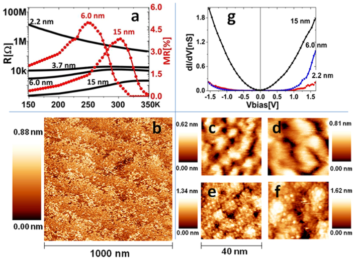
Figure 1.
(a) Resistance (R) (black curves) and magnetoresistance (MR) (red curves) versus temperature (T) for four samples of different thicknesses across the metal-insulator transition (MIT): 2.2 nm, 3.7 nm, 6 nm and 15 nm. (b) 1000 × 1000 nm2 topographic image of the 2.2-nm-thick sample (Vbias = 1.2 V, I = 0.06 nA). (c–f) 40 × 40 nm2 micrographs of the four sample thicknesses, respectively c) 2.2 nm, d) 3.7 nm, e) 6 nm and f) 15 nm. (Vbias = 1.2–0.6 V, I = 0.06–0.12 nA, depending on the sample thickness and local tunnelling conditions). (g) Room temperature differential tunnel conductivity curves measured on the three indicated samples.

