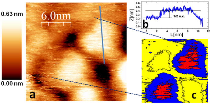
Figure 2.
(a) 20 × 20 nm2 STM micrograph of the 2.2-nm-thick sample showing a detail of the grain-like surface (Vbias = 1.2 V, I = 0.06 nA). (b) Line profile over the grain surface, indicating a step height of 0.2 nm. (c) Magnification of the image in (a), where the red to blue transition corresponds to a step height of 0.2 nm along the z-scale, revealing a defect island.

