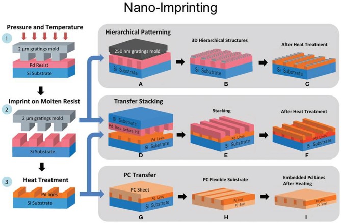
Figure 7.
Illustration of imprinting technique using a Si mold. A Pd benzylthiolate film was spin coated on Si substrate and imprinted at temperatures close to its melting point (120řC) by applying pressure. During this process, the pattern of the mold is imprinted (2) and cooled down. After de-molding (3), the patterns on the Si substrate were heat treated to obtain the final Pd patterns. During stage 2, there are a few other patterning possibilities: (A–C) hierarchical patterning can be obtained by using a different Si mold with smaller feature sizes on top of the imprinted Pd benzylthiolate patterns; (D–F) transfer stacking that is realized by using the Pd pattern and (3) as a substrate; (G–I) polycarbonate (PC) transfer that is obtained by using (3) as mold and PC as substrate. (Reprinted by permission from Macmillan Publishers Ltd: Radha et al., 2012).

