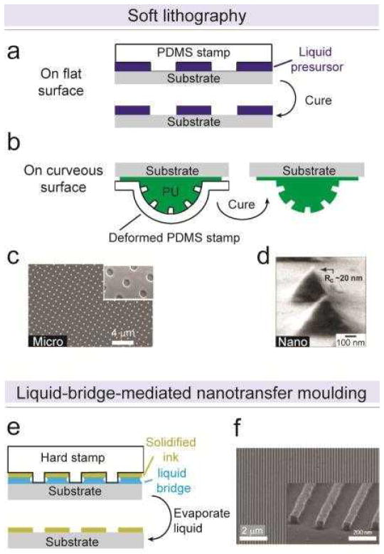
Figure 1. Fabricating micro/nanotopography in regular patterns.
(a) Schematic of fabricating micro/nano-scale structures on a flat surface using soft lithography.[38] A PDMS stamp was used to mold the liquid precursor and was peeled off after the polymer was cured. (b) Schematic of fabricating micro/nano-scale features on curvilinear surfaces using soft lithography.[61] A pre-deformed PDMS stamp was used for generating the curvilinear surface, on which secondary micro/nano-scale features were molded. (c) SEM image of microtopography fabricated by soft lithography. Reproduced with permission from [38]. Copyright 2009, Nature Publishing Group. (d) SEM image of nano-scale surface structures fabricated by soft lithography, during which an h-PDMS/PDMS composite stamp was used to facilitate high geometrical fidelity. Reproduced with permission from [60]. Copyright 2002, American Chemical Society. (e) Schematic of the liquid-bridge-mediated nanotransfer moulding (LB-nTM).[63] A hard PDMS stamp loaded with nano-patterned foreign materials was put into contact with a thin liquid layer on the substrate. When evaporating the liquid, the meniscus facilitated the transfer of nano-molded materials onto the substrate. (f) SEM image of an array of zinc-tin oxide (ZTO) nanowires transferred onto silicon substrate using LB-nTM. Reproduced with permission from [63]. Copyright 2010, Nature Publishing Group.

