
Figure 2. Fabricating micro/nanotopography in a short-range order.
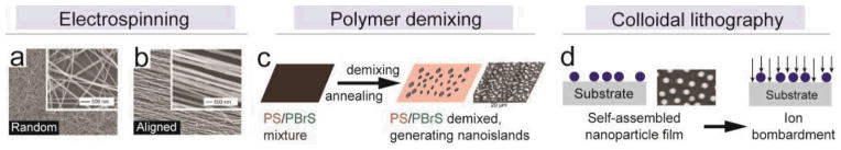
(a&b) SEM images of electrospun substrates with poly(ε-caprolactone) (PCL) nanofibers in a random (a) and highly aligned (b) fashion, respectively.[65] Reproduced with permission from [65]. Copyright 2009, Elsevier. (c) Schematic of polymer demixing and SEM image of nano-scale islands fabricated with this method.[76] PS-covered nano-islands were formed during the demixing process of a homogeneous PS/PBrS mixture undergoing annealing. Adapted with permission from [76]. Copyright 2004, Elsevier. (d) Schematic of colloidal lithography and SEM image of a self-assembled nanoparticle film used as mask for lithography.[78] The nanoparticles protected materials underneath from the ion bombardment during lithography, and thus generated nano-islands. Adapted with permission from [78]. Copyright 2003, Elsevier.