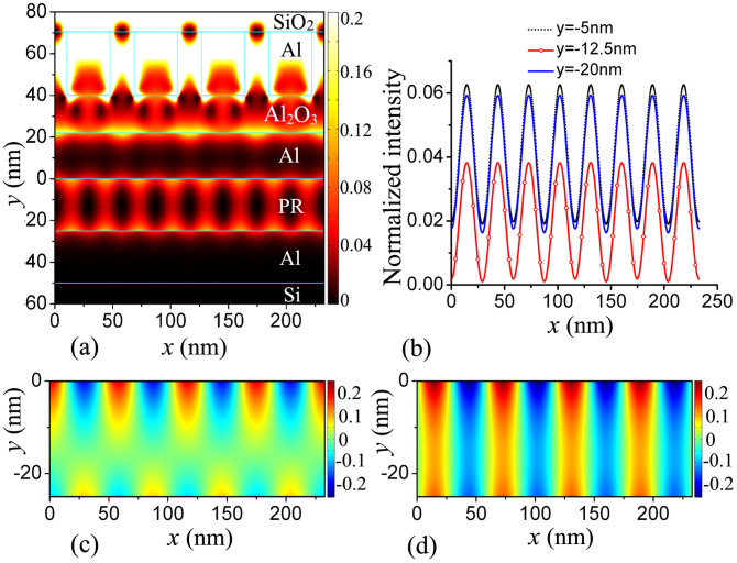
Figure 2.
(a) Normalized electric field intensity distribution of the plasmonic structure. (b) Cross sections of the normalized electric field intensity at y = −5 nm, −12.5 nm and −20 nm. (c) Distribution of normalized x component of the electric field Ex/|E0|. (d) Distribution of normalized y component of the electric field Ey/|E0|. Geometric parameters of the plasmonic structure are set as follows: Px = 58.2 nm, wx = 21 nm, d1 = 30.5 nm, d2 = 18 nm, d3 = 22 nm, d4 = 25 nm and d5 = 25 nm.

