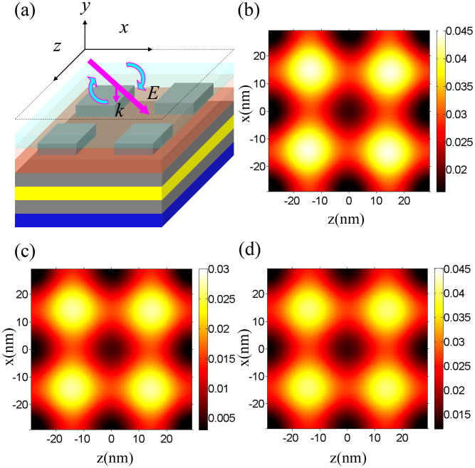
Figure 5.
(a) 3D view of the plasmonic structure. (b) Normalized electric field intensity distribution in the xz plane at y = −5 nm. (c) The same as in (b) but at y = −12.5 nm. (d) The same as in (b) but at y = −20 nm. Some parameters of the structure are set as follows: Px = Pz = 58.2 nm, wx = wz = 23 nm, d1 = 45 nm, d2 = 12 nm, d3 = 28 nm and d5 = 25 nm.

