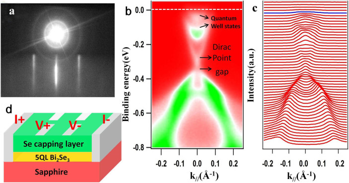
Figure 1. In situ characterizations of the 5QLs Bi2Se3 thin film grown by MBE and schematic structure for ex situ transport measurement.
(a) RHEED pattern with sharp 1 × 1 streaks. (b) ARPES band spectra along the Γ-Κ direction. The white dashed line indicates the Fermi level. The arrows label the quantum well states, the Dirac point and the small gap, respectively. (c) The corresponding momentum distribution curves of (b). The blue line indicates the Fermi level. (d) The schematic structure for transport measurements. The thickness is not to scale.

