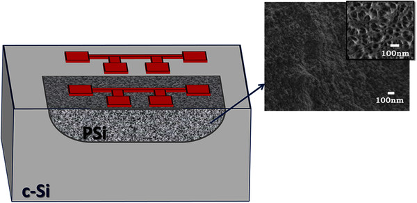
Figure 1.

Schematic representation of the test structure. The figure shows a schematic representation of the locally formed porous Si layer on the p-type wafer and SEM images of the porous Si surface. The SEM image in the inset of the principal one was obtained after a slight plasma etching of the porous Si surface in order to better reveal the porous structure. Two resistors, one on porous Si and one on bulk Si, are also depicted in the schematic of the test structure.
