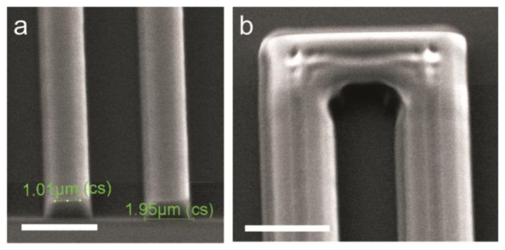
Figure 4.

SEM images (at 30° tilt) of the resist structure. (a) The 2 µm structures (resist lines represent the area between the electrodes), showing an almost 2 fold difference in the width of the top and bottom layer of the resist, with a narrower top part. The scalebar is 3 µm; (b) The resist structure at the end of an electrode, showing an inhomogeneous surface topography with a central groove. The electrode (dark region in between the light regions) is also ill-defined at the corner. The scale bar is 5 µm.
