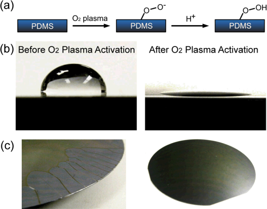
Fig. 2.
Effect of O2 plasma treatment on coating photoresist on Si wafer. (a) Surface hydrophilization of PDMS using O2 plasma treatment. (b) Contact angles of water drops on PDMS before (100°, left) and after (<5°, right) 5 min treatment of O2 plasma. (c) Images of photoresist layer spin-coated on PDMS surface with (right) and without (left) treatment O2 plasma. Photoresist could not be spread out uniformly on the PDMS surface without O2 plasma treatment (left), while after O2 plasma treatment, the photoresist could be uniformly spin-coated on PDMS.

