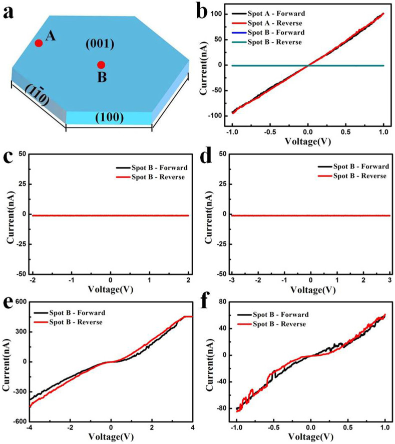
Figure 8.
(a) Schematic diagram of marked spots located in the surface of hexagonal crystal with the indexed facets. A represents fringe region, and B represents middle region. (b) I-V curves of two marked spots by C-AFM. The applied bias was swept from −1 to 1 V and reversely. (c–e) I-V curves of spot B by C-AFM. The applied bias voltages were 2 V (c), 3 V (d) and 4 V (e). (f) I-V curve of spot B by C-AFM. The applied bias voltages were reduced reversely to 1 V.

