Abstract
Metallic states appearing at interfaces between dissimilar insulating oxides exhibit intriguing phenomena such as superconductivity and magnetism. Despite tremendous progress in understanding their origins, very little is known about how to control the conduction pathways and the distribution of charge carriers. Using optical spectroscopic measurements and density-functional theory (DFT) simulations, we examine the effect of SrTiO3 (STO) spacer layer thickness on the optical transparency and carrier distribution in La δ-doped STO superlattices. We experimentally observe that these metallic superlattices remain highly transparent to visible light; a direct consequence of the appropriately large gap between the O 2p and Ti 3d states. In superlattices with relatively thin STO layers, we predict that three-dimensional conduction would occur due to appreciable overlap of quantum mechanical wavefunctions between neighboring δ-doped layers. These results highlight the potential for using oxide heterostructures in optoelectronic devices by providing a unique route for creating novel transparent conducting oxides.
High mobility two-dimensional electron gases (2DEGs) formed at atomically-well defined heterointerfaces provide an ideal platform for exploring novel quantum phenomena and developing advanced high-speed electronic devices1. Indeed the layer-by-layer growth of heterostructures with precisely-controlled chemical compositions at the atomic scale have opened the door to the artificial design of interface-engineered heterostructures; an advancement at the core of the semiconductor industry2. A prominent discovery, borne out of such an interface-engineered heterostructure, is the presence of a 2DEG3. In semiconductors, 2DEGs reveal extremely high mobility, especially, at low temperatures. Furthermore, they reside at quantized energy levels and, therefore, offer many intriguing quantum phenomena, such as the quantum Hall effect1,4 and the fractional quantum Hall effect5. 2DEGs derived from transition-metal oxide heterostructures would offer another degree of freedom for manipulating the electrical properties through the strong correlations of d-band electrons.
Recently, it has been demonstrated that such a 2DEG6,7,8 could be created in an oxide heterostructure through interfacial electronic reconstruction9 or the introduction of oxygen vacancies at the STO surface10,11,12. The former includes a heterostructure composed of the Mott insulator LaTiO3 (LTO) and the band insulator STO, which generates a high-density of carriers, up to 0.5 electrons per unit cell area or n2D ~ 3 × 1014 cm−2 (Ref. 13), with transport that occurs along multiple channels resulting in high mobility through alleviated transport bottlenecks in a superlattice structure14. These features offer tremendous promise for realizing oxide electronics15 or photovoltaics16 with 2DEGs. However, the spatial extent of the conducting carriers away from the interfaces in a short-period superlattice has not been fully explored. Despite an early scanning transmission electron microscopy (STEM)-electron energy loss spectroscopy (EELS) study by Ohtomo et al.6, which demonstrated that the spatial extent of the electron distribution was ~2 nm or ~5 unit cells (u.c.) away from the interface at room temperature, very little effort has been focused on understanding the consequences of this leakage for electronic transport within a superlattice.
In this regard, δ-doped superlattices present the ideal framework for understanding the electronic reconstruction that can occur at oxide interfaces, both from theory and experiment13,17,18. For example, we recently demonstrated that by controlling the fraction of “dopant” ions at the interface one can achieve a significant enhancement in the mobility of the carriers at an interface18. Moreover, since the effects are purely driven by chemistry, physical mechanisms such as the polar-catastrophe do not apply and thus it is possible to explore the effects of the thickness of the insulating layer (i.e. STO) using standard experimental geometries. From the perspective of theory, it reduces the size of the system that has to be modeled, thus allowing for a more straightforward determination of the electronic structure.
Here, we investigate the effect of the STO insulating layer thickness on the optical properties and electronic structures of La δ-doped STO superlattices. Using atomically controlled superlattices, we experimentally show that these materials remain highly transparent to visible light, irrespective of STO spacer thicknesses. Our DFT calculations, indicate that this is a direct consequence of minimal changes in the band gap between O 2p and Ti 3d states. Furthermore, using DFT we examine the effect of STO layer thickness on the amplitude of charge density in the STO spacer region due to the overlap of the wavefunctions permeating from neighboring, conductive δ-doped layers. Our results for thinner STO spacers indicate a clear crossover from 2D carrier density profiles to 3D, with the emergence of a single electronic band with light effective mass. This may be indicative of enhanced conductivity perpendicular to the interface. Together, these results illustrate that it is possible to create a 3D, transparent conducting oxide by engineering the wavefunction of 2D materials. These results have importance for building design concepts for tuning the properties at oxide interfaces; with particular consequences for the field of mesoscale optoelectronics.
Results
Optical properties
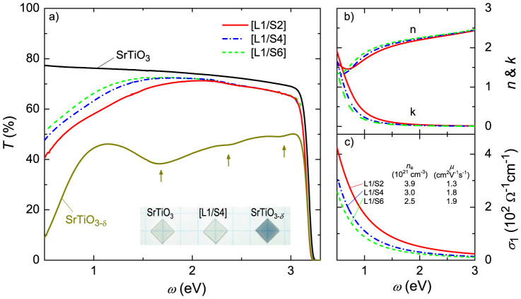
Typically, doped conducting transition-metal oxides, for instance La-, Nb-, or oxygen vacancy-doped STO, have high light-absorption due to accompanying defects and/or deep-level impurities19,20, resulting in significant opacity (e.g., see the inset of Figure 1a). As such transition-metal oxides with partially filled d-band electrons are generally considered to be poor candidates for transparent conducting oxides (TCOs). However, LTO/STO superlattices with electronically-reconstructed interfaces represent completely different band structures as compared to those of chemically-doped STOs, which typically create in-gap states21. Figure 1a depicts the optical transmittance (T) for [L1/S2], [L1/S4] and [L1/S6] superlattices grown by pulsed laser deposition (PLD) on TiO2-terminated (001) STO single crystal substrates (i.e. STO spacer thicknesses of 2, 4 and 6 layers, respectively). Similar to an undoped STO crystal, all of the La δ-doped STO superlattices are transparent in the visible range, while showing clear evidence of conducting carriers, i.e., the Drude absorption, in the low photon energy region (<1.5 eV). Using a simple Drude model fit, we have calculated the extinction coefficient (k) of the complex refractive index (ň = n + ik) as a function of photon energy. This fit confirms that the δ-doped superlattices remain transparent in the visible range (Figure 1b). Note that the higher interface density in the [L1/S2] superlattices results in lower transmittance as compared to the longer period superlattices (Figure 1). It is worth noting that both the measured transmittance and resistivity of the superlattices are comparable to those of the most widely used TCO, i.e. Sn-doped In2O3 (ITO) (T = 80%, ρ = 200 μΩ·cm)22, and the superlattices' room-temperature carrier mobility is also comparable to that of ITO as we reported elsewhere13,14.
Figure 1.
(a) Optical transmittance (T) of the [L1/S2], [L1/S4] and [L1/S6] superlattices (60 nm in total thickness) on STO substrates as a function of photon energy (ω). Optical spectra for an undoped bare STO substrate and an oxygen-vacancy-doped STO film (100 nm thick) on STO are also shown for comparison. Superlattice samples clearly show the Drude absorption and no noticeable absorption due to in-gap states. Inset: Photographs of a bare STO substrate, [L1/S4], and oxygen-vacancy-doped STO film. The oxygen-vacancy-doped STO absorbs a significant portion of visible light with clear evidence of in-gap defect states, as marked with arrows. (b) Extinction coefficient (k) and refractive index (n), and (c) optical conductivity (σ1) of the [L1/S2], [L1/S4] and [L1/S6] superlattices obtained from a Drude fit to the experimental transmittance data. The net carrier density and mobility for each sample are listed for convenience. For all three samples the carrier density is within experimental error bars of 0.5 e−/interface13,14.
As evident from the density of states (DOS) shown in Figure 2, δ-doped superlattices have their Fermi levels residing within the Ti bands and the gap between the O 2p states and Ti 3d-t2g states (the allowed optical transition) remains, relatively, the same as in undoped STO. As such, these materials should be transparent to visible light. (N.B.: Our DFT calculations underestimate the band gap; thus, even though they are smaller than the required 3 eV, the results are consistent with a material that would be optically transparent). This is unlike the O-deficient SrTiO2.875, where bulk dopants result in the narrowing of the band gap through the creation of in-gap states (see Figure 2 and 3b). Additionally, analysis of the band structure (Figure 3c and d) shows that the transitions from the conduction states to higher lying unoccupied 3d-states are ~2 eV or less, consistent with the Drude feature observed experimentally (Figure 1a).
Figure 2. DOS calculated for undoped STO, O-deficient SrTiO2.875, [L1/S2], and [L1/S6].
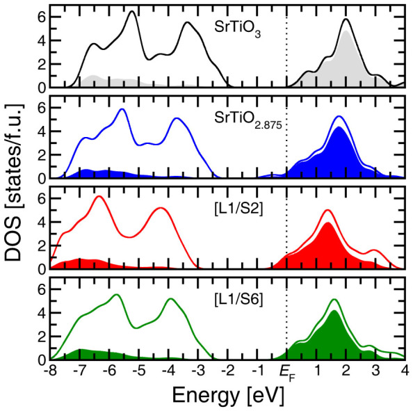
The solid lines and shaded areas represent the total DOS and projected DOS for Ti 3d-states, respectively.
Figure 3.
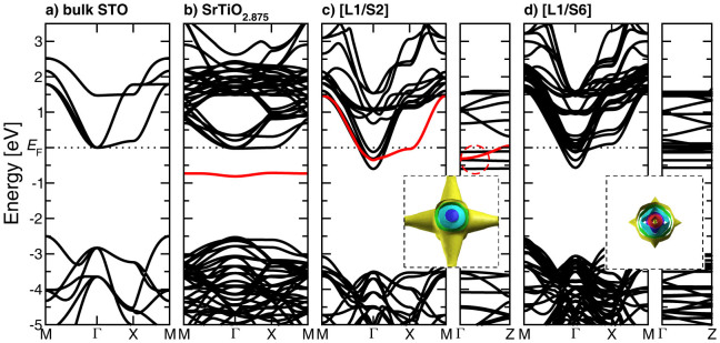
Electronic band structure for (a) bulk STO, (b) an O-vacancy in SrTiO2.875, (emphasizing the in-gap state in red), (c) [L1/S2] and (b) [L1/S6]. The partially occupied states near the Fermi level, EF, and the change in dispersion along the Γ-Z direction in the [L1/S2] superlattice are highlighted in red. Inset: Fermi-surface for each system, representing 3D and 2D conduction of interfacial charge carriers, respectively. Fermi-surface plots in the XY and XZ planes are included in the Supplementary Information.
Electronic reconstruction
While these superlattices have very similar optical properties, their electronic properties could be very different. Indeed, we know from experiment that the spatial extent of the electrons is roughly 3–5 unit cells6,9,23 away from the interface which could result in significant overlap in the carrier densities in superlattices with thinner STO spacer regions. In order to fully explore the dimensional behavior, we examine the spatial distribution of the 2DEG carrier densities as a function of STO thickness. To compute the number of electrons that contribute to the 2DEG carrier density, we sum up the atomic projected DOS for the partially occupied states just below the Fermi level, EF (see Figure 3). In agreement with previous studies, for all three superlattices, the total DOS sums up to exactly 1 electron (or rather 0.5 e−/interface)24,25,26. (Note: Due to the integration sphere for computing the atom projected DOS, the partial DOS for the [L1/S2], [L1/S6] and [L1/S10] sum up to 0.95 electrons.) As seen in Figure 4c, in the [L1/S10] superlattice, the extra electron due to the electronic reconstruction is adequately screened in the bulk of STO, indicating that the accumulated charge extends to roughly 3 unit cells away from the interface. Similar results are observed for the [L1/S6] superlattice (Figure 4b). However, in this case, while there is a substantial drop in the charge density profile away from the interface, the relatively thinner STO layers in the [L1/S6] system allow for some wavefunction overlap and therefore the charge density does not completely disappear as in the [L1/S10] superlattices. These results are in good agreement with previous theory and experiment9,11,24,25,26,27,28,29.
Figure 4.
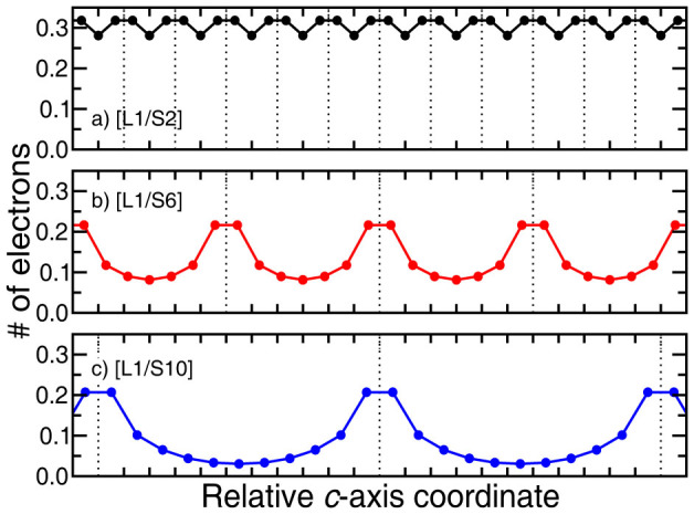
Charge distribution as a function of the relative c-axis coordinate for the (a) [L1/S2], (b) [L1/S6] and (c) [L1/S10] superlattices. Dotted lines indicate the position of the LaO planes and each tick along the x-axis represents one perovskite unit-cell.
Moreover, the spatial distribution of the electrons is expected to play an important role in controlling transport away from the oxide interface in superlattices with shorter STO spacer regions. Indeed in the [L1/S2] superlattice, the wavefunction overlap results in very little change in the total number of conduction electrons within the STO layers (Figure 4a). This charge density profile indicates that the conductivity in the direction perpendicular to the oxide interface. A detailed comparison of the electronic band structure of the [L1/S2] and [L1/S6] heterostructures reveals two important features (as shown in Figure 3). First, we observe a significant difference in the Fermi surfaces (FS) of the two systems. Specifically, we find an increased FS volume in the [L1/S2] superlattice. Four rods extending along the Γ-X and the Γ-Y directions indicate the large contribution from dxz and dyz states. Second, this increased FS volume is accompanied by the population of a light electron effective mass band in the Γ-Z direction again originating from the dxz and dyz states (as determined from a k-resolved DOS analysis; see Supplementary Information Figure S1). These two features point to enhanced mobility in the out-of-plane direction; signaling a crossover from 2D to 3D conductivity.
Experimentally, angle-dependent Shubnikov de Haas (SdH) oscillations can be used to confirm the dimensional crossover from 2D to 3D conductivity; with the oscillations disappearing in the 2D conducting case as the angle is rotated away from the kx-ky plane19,20,27,28. However, while resistivity measurements clearly show that the samples are highly conducting, we were unable to observe SdH oscillations in our samples even at temperatures down to 25 mK and magnetic fields up to 35 T. It is important to note the large FS cross-sectional areas computed for the [L1/S2] superlattice (5.43 nm−2 for the smallest FS) and the [L1/S6] superlattice (5.84 and 0.76 nm−2 for the two smallest FS). (FS areas were computed as circles with a radius along the Γ-M direction.) These FS areas are much larger than the previously reported experimental values for Nb δ-doped STO (0.36 nm−2)29 and La-doped STO thin films (0.26 nm−2)17 and are in fact on the order of the FS cross-sectional areas found in YBa2Cu3O6.5 (5.1 nm−2)30,31. Of course, as the [L1/S6] superlattice includes some smaller FS areas that are on the order of those in Nb/La-doped STO, we should expect to observe SdH oscillations in these samples. However, we believe that the contributions from the larger FS may suppress the SdH oscillations. This large FS size suggests that it may be only possible to observe angle-dependent SdH oscillations in our superlattices at much higher magnetic fields.
Naturally, localization effects are crucial to defining the mobility of electrons at oxide heterointerfaces. Tight-binding simulations show that at dissimilar interfaces there is a strong reduction of the in-plane hopping amplitude of the dxz and dyz orbitals24,32; driving the dxy orbital ordering. Thus, the dxy orbitals become extremely localized; severely limiting electron mobility in these orbitals. In the two carrier model, the latter states have a high density, but low mobility (HDLM; nS = 0.4 ~ 1 × 1016 cm−2 and μ = 10 ~ 50 cm2/Vs at 2 K) while carriers in the dxz and dyz orbitals have low densities but high carrier mobilities (LDHM; nS = 0.2 ~ 1 × 1013 cm−2 and μ = 1,000 ~ 5,000 cm2/Vs at 2 K)14.
To better understand the effects of delocalization due to enhanced wavefunction overlap, we compute the fractional occupation, f, of the dxz/yz vs. dxy orbitals:
 |
where ni (i = xz, yz or xy) is the number of electrons in the dxz, dyz or dxy orbital, respectively. As depicted in Figure 5, it is clear that the reduction in STO thickness results in a substantial increase in the relative fraction of dxz/yz orbitals at the heterostructure interface. Assuming that these states remain mostly delocalized, this would suggest higher mobility at these interfaces. Similar effects are likely the cause of the anomalous enhancement in mobilities in the previously studied δ-doped oxide superlattices18. Interestingly, we find that the number of dxy electrons, nxy, at the interface remains constant in the [L1/S2] and [L1/S6] superlattices (See Supplementary Information Figure S2), and the large change in fractional occupation at the interface is a consequence of an increase in dxz and dyz populations.
Figure 5.
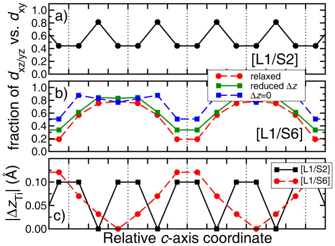
Fractional occupations of dxz/yz orbitals versus dxy as a function of the relative c-axis coordinate for (a) [L1/S2] and (b) [L1/S6]. (c) The magnitude of the Ti displacements, |ΔzTi|, away from the La δ-doped layer. Coordinates are relative to the LaO plane and dashed lines indicate the position of the LaO planes in each system.
Commensurate with these changes in the relative populations of the dxz/dyz orbitals, we observe significant differences in the off-center displacements relative to their nearest neighbor oxygen octahedral cage, Δz, of Ti cations; with the [L1/S6] superlattices exhibiting larger off-centering than the [L1/S2] superlattices. Off-centering is known to be coupled to a larger distribution in electron densities away from the interface. We find that if the off-center displacements in the [L1/S6] superlattice are manually reduced to that of the [L1/S2] superlattice (Figure 5b; reduced Δz) there is a ~50% increase in the relative populations of the dxz/yz orbitals. This increase in relative populations is even more dramatic when the off-center displacements are completely eliminated (Figure 5b; Δz = 0). Again, we find that the number of dxy carriers remains relatively constant, while the excess electrons at the interface now occupy the previously low-density dxz/yz orbitals.
These results emphasize the role of the confinement of electrons near the interface, which results in the population of the high mobility carriers, dxz/yz carrier. Furthermore, the fact that the [L1/S2] superlattice has a smaller displacement and a larger carrier density suggests that electronic screening may play a substantial role in the [L1/S2] superlattice; with the superlattice having a smaller effective dielectric constant than that of the [L1/S6] superlattice. Similar results were obtained using model Hamiltonian studies33,34 and hypothesized as the origin of the predicted difference in the distribution of electrons in the δ-doped KTaO3 and KNbO3 systems25. It should be noted that the overall mobility at the interface may be affected by other factors such as carrier interactions at the interface and interface scattering. Nevertheless, the interconnection of the high mobility 2DEGs generated by the interfacial electronic reconstruction and changes in the effective dielectric constant at these interfaces may provide an unprecedented pathway for designing a new class of highly metallic, transparent conducting oxides.
Summary
We have investigated the dimensional nature of carrier distribution and optical transport in electronically-reconstructed interfaces via DFT calculations. It has been found that there is a dimensional crossover of carrier conduction from 2D to 3D with a critical STO thickness of ~2–3 nm in thickness. This dimensional crossover is attributed to a significant overlap of quantum mechanical wavefunctions inside the STO matrix when the distance between neighboring conducting layers is thin enough, implying that the wavefunction of oxide superlattices might be engineered by means of structural modifications, dielectric property, and electric field. Even more striking, the electronically reconstructed metallic interfaces uniquely transmit visible light offering a new mechanism for developing transparent conducting films. In essence, by decoupling the dopants from the optically transparent layers it is possible to retain the favorable band gap of STO without introducing in gap states. Considering these unique properties such as tunable electronic wavefunctions and optical transparency, the oxide superlattice is promising for the development of novel optoelectronic devices where the interactions between photons and electrons are critical to the functional behavior of these materials.
Methods
All DFT calculations were performed using ultrasoft pseudopotentials with the local density approximation (LDA) for exchange and correlation as implemented in the quantum espresso35 simulation code. LTO/nSTO [L1/Sn] superlattices (where n = 2, 6 and 10) were studied employing a 500 eV cutoff and a 16 × 16 × 1 Monkhorst-Pack k-point mesh with 1 × 1 unit cell in-plane periodicity. In all calculations, the in-plane lattice constants were constrained to the theoretical value of STO (3.863 Å) and the out-of-plane, c, lattice vector was optimized within the P4mm space group. Simultaneously, all ionic coordinates were relaxed until all Hellman-Feynman forces were less than 5 meV/Å. Note that the cubic STO lattice constant was obtained using standard LDA, i.e. without the inclusion of a Hubbard U (Ref. 36) and is in typical LDA agreement with the experimental value of 3.901 Å. For all heterostructure calculations, a Hubbard U = 5 eV for Ti 3d-states was found to be appropriate. Similar U values have been used in previous studies of LTO/STO18,24,25,26 and have been shown to give a reasonable description of the electronic and structural rearrangements that occur in these materials.
La δ-doped STO superlattices were grown on TiO2-terminated (001) STO single crystal substrates by PLD (KrF, λ = 248 nm) using polycrystalline La2Ti2O7 and single crystalline STO targets. The thickness of each layer was monitored in-situ by reflection high-energy electron diffraction (RHEED). During the growth of STO, we inserted one u.c. LTO with various thicknesses of STO spacers ranging from 2 to 10 u.c., resulting in La δ-doped STO superlattices. The total thickness of superlattices ranged from 30–60 nm. Detailed growth conditions and structural properties can be found elsewhere13,14,18. Quantum transport properties of the superlattices were investigated at temperatures down to 25 mK and magnetic fields up to 35 T. Under these conditions no noticeable quantum oscillations were observed.
Author Contributions
V.R.C. performed the DFT calculations. V.R.C. and S.O. analyzed the theoretical results. S.L. performed the quantum transport measurements and data analysis at ORNL. S.S.A.S. carried out optical characterization and analysis. J.S.K. and W.S.C. assisted with measurements and analysis of the dc transport and optical properties. H.N.L. designed the project, coordinated the work, and assisted with sample synthesis and analysis. All authors participated in discussions and manuscript writing.
Supplementary Material
Supplementary Information
Acknowledgments
The authors thank Y. Lee and L. Balicas for experimental assistance, P. D. C. King for helpful discussions and N. Sivadas for technical assistance. This work was supported by the U.S. Department of Energy, Basic Energy Sciences, Materials Sciences and Engineering Division (V.R.C., W.S.C., S.S.A.S., S.O., H.N.L.), and the Office of Science Early Career Research Program (V.R.C.). S.L. was supported by the Korea Institute of Science and Technology (KIST) through Grant No. 2E24001. This research used resources of the National Energy Research Scientific Computing Center, supported by the Office of Science, U.S. Department of Energy under Contract No. DEAC02-05CH11231.
References
- Ando T., Fowler A. B. & Stern F. Electronic properties of two-dimensional systems. Rev. Mod. Phys. 54, 437–672 (1982). [Google Scholar]
- Grahn H. T. Semiconductor Superlattices. (World Scientific, 1995). [Google Scholar]
- Dingle R., Stormer H. L., Gossard A. C. & Wiegmann W. Electron mobilities in modulation-doped semiconductor heterojunction superlattices. Appl. Phys. Lett. 33, 665–667 (1978). [Google Scholar]
- v. Klitzing K., Dorda G. & Pepper M. New method for high-accuracy determination of the fine-structure constant based on quantized Hall resistance. Phys. Rev. Lett. 45, 494–497 (1980). [Google Scholar]
- Tsukazaki A. et al. Quantum Hall effect in polar oxide heterostructures. Science 315, 1388–1391 (2007). [DOI] [PubMed] [Google Scholar]
- Ohtomo A., Muller D. A., Grazul J. L. & Hwang H. Y. Artificial charge-modulationin atomic-scale perovskite titanate superlattices. Nature 419, 378–380 (2002). [DOI] [PubMed] [Google Scholar]
- Ohtomo A. & Hwang H. Y. A high-mobility electron gas at the LaAlO3/SrTiO3 heterointerface. Nature 427, 423–426 (2004). [DOI] [PubMed] [Google Scholar]
- Shibuya K., Ohnishi T., Kawasaki M., Koinuma H. & Lippmaa M. Metallic LaTiO3/SrTiO3 superlattice films on the SrTiO3 (100) surface. Jpn. J. Appl. Phys. 43, L1178–L1180 (2004). [Google Scholar]
- Okamoto S. & Millis A. J. Electronic reconstruction at an interface between a Mott insulator and a band insulator. Nature 428, 630–633 (2004). [DOI] [PubMed] [Google Scholar]
- Herranz G. et al. High mobility in LaAlO3/SrTiO3 heterostructures: Origin, dimensionality, and perspectives. Phys. Rev. Lett. 98, 216803 (2007). [DOI] [PubMed] [Google Scholar]
- Santander-Syro A. F. et al. Two-dimensional electron gas with universal subbands at the surface of SrTiO3. Nature 469, 189–193 (2011). [DOI] [PubMed] [Google Scholar]
- Meevasana W. et al. Creation and control of a two-dimensional electron liquid at the bare SrTiO3 surface. Nat. Mater. 10, 114–118 (2011). [DOI] [PubMed] [Google Scholar]
- Seo S. S. A. et al. Optical study of the free-carrier response of LaTiO3/SrTiO3 superlattices. Phys. Rev. Lett. 99, 266801 (2007). [DOI] [PubMed] [Google Scholar]
- Kim J. S. et al. Nonlinear Hall effect and multichannel conduction in LaTiO3/SrTiO3 superlattices. Phys. Rev. B 82, 201407(R) (2010). [Google Scholar]
- Mannhart J. & Schlom D. G. Oxide interfaces - An opportunity for electronics. Science 327, 1607–1611 (2010). [DOI] [PubMed] [Google Scholar]
- Assmann E. et al. Oxide heterostructures for efficient solar cells. Phys. Rev. Lett. 110, 078701 (2013). [DOI] [PubMed] [Google Scholar]
- Jalan B., Stemmer S., Mack S. & Allen S. J. Two-dimensional electron gas in δ-doped SrTiO3. Phys. Rev. B 82, 081103 (2010). [Google Scholar]
- Choi W. S., Lee S., Cooper V. R. & Lee H. N. Fractionally δ-doped oxide superlattices for higher carrier mobilities. Nano Lett. 12, 4590–4594 (2012). [DOI] [PubMed] [Google Scholar]
- Lee C., Destry J. & Brebner J. L. Optical absorption and transport in semiconducting SrTiO3. Phys. Rev. B 11, 2299–2310 (1975). [Google Scholar]
- Baer W. S. Free-carrier absorption in reduced SrTiO3. Phys. Rev. 144, 734–738 (1966). [Google Scholar]
- Kim Y. S. et al. Localized electronic states induced by defects and possible origin of ferroelectricity in strontium titanate thin films. Appl. Phys. Lett. 94, 202906 (2009). [Google Scholar]
- Ishibashi S., Higuchi Y., Ota Y. & Nakamura K. Low resistivity indium in oxide transparent conductive films. II. Effect of sputtering voltage on electrical property of films. J. Vac. Sci. Technol., A 8, 1403–1406 (1990). [Google Scholar]
- Cantoni C. et al. Electron transfer and ionic displacements as the origin of the 2D electron gas at the LAO/STO interface: Direct measurements with atomic-column spatial resolution. Adv. Mater. 24, 3952–3957 (2012). [DOI] [PubMed] [Google Scholar]
- Okamoto S., Millis A. J. & Spaldin N. A. Lattice relaxation in oxide heterostructures: LaTiO3/SrTiO3 superlattices. Phys. Rev. Lett. 97, 056802 (2006). [DOI] [PubMed] [Google Scholar]
- Cooper V. R. Enhanced carrier mobilities in two-dimensional electron gases at III-III/I-V oxide heterostructure interfaces. Phys. Rev. B 85, 235109 (2012). [Google Scholar]
- Hamann D. R., Muller D. A. & Hwang H. Y. Lattice-polarization effects on electron-gas charge densities in ionic superlattices. Phys. Rev. B 73, 195403 (2006). [Google Scholar]
- Isihara A. & Smrcka L. Density and magnetic field dependences of the conductivity of two-dimensional electron systems. J. Phys. C: Solid State Phys. 19, 6777–6789 (1986). [Google Scholar]
- Averkiev N. S., Golub L. E. & Tarasenko S. A. Quasi-two-dimensional Shubnikov-de Haas effect. J. Exp. Theor. Phys. 90, 360–362 (2000). [Google Scholar]
- Kozuka Y. et al. Two-dimensional normal-state quantum oscillations in a superconducting heterostructure. Nature 462, 487–490 (2009). [DOI] [PubMed] [Google Scholar]
- Doiron-Leyraud N. et al. Quantum oscillations and the Fermi surface in an underdoped high-Tc superconductor. Nature 447, 565–568 (2007). [DOI] [PubMed] [Google Scholar]
- Barisic N. et al. Universal quantum oscillations in the underdoped cuprate superconductors. Nat. Phys. 9, 761–764 (2013). [Google Scholar]
- Khalsa G., Lee B. & MacDonald A. H. Theory of t2g electron-gas Rashba interactions. Phys. Rev. B 88, 041302(R) (2013). [Google Scholar]
- Okamoto S. & Millis A. J. Theory of Mott insulator-band insulator heterostructures. Phys. Rev. B 70, 075101 (2004). [Google Scholar]
- Kancharla S. S. & Dagotto E. Metallic interface at the boundary between band and Mott insulators. Phys. Rev. B 74, 195427 (2006). [Google Scholar]
- Giannozzi P. et al. QUANTUM ESPRESSO: a modular and open-source software project for quantum simulations of materials. J. Phys.: Condens. Matter 21, 395502 (2009). [DOI] [PubMed] [Google Scholar]
- Anisimov V. I., Zaanen J. & Anderson O. K. Bond theory and Mott insulators: Hubbard U instead of Stoner T. Phys. Rev. B 44, 943–954 (1991). [DOI] [PubMed] [Google Scholar]
Associated Data
This section collects any data citations, data availability statements, or supplementary materials included in this article.
Supplementary Materials
Supplementary Information


