
Figure 3.
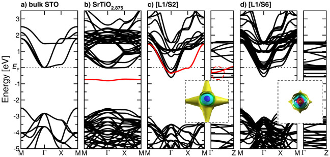
Electronic band structure for (a) bulk STO, (b) an O-vacancy in SrTiO2.875, (emphasizing the in-gap state in red), (c) [L1/S2] and (b) [L1/S6]. The partially occupied states near the Fermi level, EF, and the change in dispersion along the Γ-Z direction in the [L1/S2] superlattice are highlighted in red. Inset: Fermi-surface for each system, representing 3D and 2D conduction of interfacial charge carriers, respectively. Fermi-surface plots in the XY and XZ planes are included in the Supplementary Information.