Nano- and meso-scale photoactive structures are central to a number of light-conversion technologies, including photovoltaics and catalysts for solar hydrogen production.[1] Often, these applications involve the use of a wide-band-gap semiconductor such as TiO2 or ZnO to transport photogenerated charges and impose mesostructure. While these materials are convenient structural scaffolds and efficient charge-transport materials, they must be sensitized with a thin layer of a narrow-band-gap absorber to efficiently harvest incident light. Such systems form the basis of dye-sensitized and semiconductor-sensitized solar cells (DSSC and SSSC, respectively), in which photogenerated electrons in the sensitizer are transferred to, and subsequently transported through, a porous metal oxide.[2] The associated holes are transferred to a liquid electrolyte or a solid hole transport material (HTM). A disadvantage of this configuration is the energetic cost inherent to the transfer of photoexcited electrons and holes from the sensitizer, which limits open circuit voltage. Furthermore, metal-oxide films must be thick enough for sufficient light absorption by the thin sensitizer layer. Increasing film thickness raises the probability of charge recombination and can restrict uniform penetration of a solid-state HTM. Such issues can be addressed by employing a single material that combines the electrical, optical, and structural functions of the sensitized metal oxide as a light-harvesting photoanode, where charge separation is instigated by hole transfer to an HTM, and photogenerated electrons are transported through the absorber material. Metal sulfides and selenides are promising candidates to fulfill this multifaceted role, with large extinction coefficients and red-shifted absorption onsets reported for a wide range of materials, as well as high electrical conductivities. However, a key requirement is the ability to control the morphology of the absorbing material to maximize the yield of charge separation at the absorber/HTM interface while maintaining electrical conductivity. Herein, we introduce a strategy for the low-temperature, solution-based preparation of photosensitive, mesoporous metal–chalcogenide films from a printable metal–xanthate-based paste. The size of the absorber crystals, and thus the size of the pores in the film, can be controlled by variation of the temperature at which the precursor layer is annealed. We consider the potential of these films for use in hybrid organic-inorganic solar cells by filling the pores with an organic polymer. Transient absorption spectroscopy reveals that charge separation does take place by hole transfer at the inorganic–organic heterojunction. Preliminary photovoltaic devices demonstrate short-circuit currents of almost 5 mA cm−2, indicating that the Sb2S3 crystals are electrically connected and able to transport photogenerated charge.
The use of metal xanthates and similar complexes as thermally decomposable precursors to metal sulfides is well established.[3] In the context of photovoltaics, we and other groups have previously used this process in the preparation of nanostructured metal sulfide/polymer blends for use as inorganic–organic hybrid solar cell active layers,[4] as well as to photosensitize mesoporous TiO2 for SSSC-type heterojunctions.[5] Herein, we describe a general approach to the preparation of mesoporous metal–chalcogenide films from a printable metal–xanthate precursor paste. As a proof of concept, we apply this to the decomposition of an antimony triethyldithiocarbonate precursor (antimony ethyl xanthate, [Sb(EX)3]; Scheme 1) to form porous crystalline Sb2S3 films. A high extinction coefficient (1.8×105 cm−1 at 450 nm) and a bandgap of ca. 1.7–1.8 eV make Sb2S3 a particularly attractive photovoltaic material,[6] which has led to its use as an absorber material in a range of solar power devices, including thin film,[7] semiconductor-sensitized,[8] and hybrid organic–inorganic solar cells.[4d] Our recent study on Sb2S3-sensitized solar cells has indicated that charge separation can be instigated by hole transfer to an organic hole conductor,[9] while our work on Sb2S3–polymer blend hybrid systems has demonstrated its ability to conduct photogenerated electrons.[4d] As such, Sb2S3 is a very promising candidate to undertake the dual role of light absorption and charge transport required of a light-harvesting photoanode. To form mesoporous films of Sb2S3, a precursor paste was prepared by adding a small amount of hexylamine to a chlorobenzene solution containing [Sb(EX)3]. Alkylamines have previously been reported to promote the decomposition of metal xanthates, potentially through nucleophilic attack of the (thio)carbonyl center.[10] Furthermore, we have recently shown that sacrificial amine additives can be used to modulate the crystallinity of CdS nanocrystals that were grown by metal xanthate decomposition in a polymer matrix.[11] In the present work, addition of the amine causes the pale yellow xanthate solution to become dark brown/orange and viscous, thus indicating at least partial decomposition of the precursor (Scheme 1). The paste is doctor bladed to form an orange precursor layer on a glass or conducting glass substrate, and subsequently thermally annealed in a nitrogen glove box, becoming grey and highly optically scattering in the process. Figure 1 a shows the absorption spectra of a glass slide coated with the precursor layer before (grey) and after (black) thermal annealing at 120 °C. For the annealed film, the absorption onset at ca. 740 nm is consistent with the bandgap of crystalline antimony sulfide (1.7–1.8 eV).[6] The composition of the annealed film is confirmed by X-ray diffraction (Figure 1 b), which displays the characteristic peaks of the stibnite mineral (ICDB reference pattern 00-042-1393). Figure 1 c is a cross-sectional scanning electron micrograph of the Sb2S3 layer on a fluorine-doped tin oxide substrate, showing a mesoporous film of Sb2S3 that is ca. 400–500 nm thick. Additional evidence for the formation of pure Sb2S3 is given by core-level X-ray photoelectron spectroscopy (XPS; see the Supporting Information). Importantly, XPS confirms the presence of nitrogen in the precursor layer, but not after thermal annealing. This indicates that the amine does not remain bound to the antimony sulfide, but rather acts as a processing additive. Moreover, the narrow core-level antimony 3d and sulfur 2p XPS peaks for the annealed film indicate complete conversion of the precursor into Sb2S3.
Scheme 1.
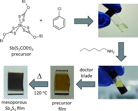
The processing of antimony ethylxanthate into mesoporous films of Sb2S3.
Figure 1.
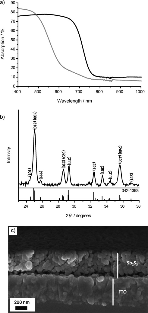
a) Absorption spectra of an [Sb(EX)3] film as deposited (grey) and after annealing at 120 °C in a nitrogen-filled glovebox (black). b) X-ray diffraction pattern of an Sb2S3 film after annealing at 120 °C in a nitrogen-filled glovebox. c) Scanning electron micrograph showing the cross-sectional profile of the Sb2S3 deposit (annealed at 160 °C).
We now demonstrate that it is possible to control the size of the Sb2S3 crystals and the porosity of the resulting films through the temperature at which the [Sb(EX)3] precursor layer is annealed. Figure 2 a shows the variation in full-width half-maximum (FWHM) of the (211) peak from the Sb2S3 X-ray diffraction pattern, and corresponding average crystallite sizes calculated using the Scherrer formula, as a function of annealing temperature. The corresponding raw spectra are included in the Supporting Information. Peak sharpness is seen to increase at higher annealing temperatures, which indicates an increase in average crystallite size. In a similar fashion, top-down scanning electron micrographs reveal a dramatic increase in particle size with increased annealing temperature (Figure 2 b–d). At the lower temperature, a relatively homogeneous film of sub-100 nm crystals is observed, whereas at 160 °C, there is a mixture of the smaller crystals with platelets ca. 200 nm in size. As the annealing temperature is increased further, the number of smaller crystals decreases, leading to a greater average crystallite size and larger pores.
Figure 2.
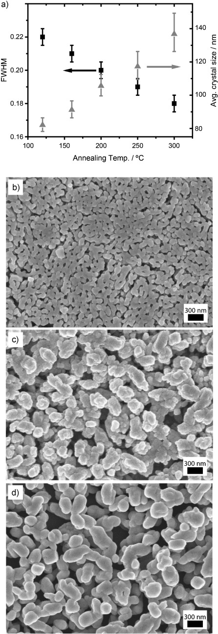
a) Full-width at half-max (FWHM) of the Sb2S3 (211) X-ray diffraction peak and corresponding average crystallite size in this plane, as calculated by the Scherrer equation, as a function of annealing temperature. b) Top-down scanning electron micrograph of an FTO/Sb2S3 film, following annealing at 120 °C. c) Top-down SEM of an FTO/Sb2S3 film, following annealing at 160 °C. d) Top-down SEM of an FTO/Sb2S3 film, following annealing at 300 °C.
The porous nature of the Sb2S3 films shown in Figure 2 provides a large surface area and therefore the potential for efficient interfacial charge separation in the presence of a suitable acceptor material. To assess this, we spin-coat poly-3-hexylthiophene (P3HT) into the pores of the annealed Sb2S3 films and use microsecond-millisecond transient absorption spectroscopy to probe charge separation across the Sb2S3/P3HT heterojunction. As the absorption profiles of Sb2S3 and P3HT strongly overlap at about 500–640 nm (see the Supporting Information), we excite the composite layer at 650 nm. In this manner, the contribution of the inorganic component is primarily probed, rather than potential charge transfer from P3HT to Sb2S3. Figure 3 a shows the transient absorption spectrum of a typical Sb2S3/P3HT composite 1 μs after pulsed photoexcitation. The shape of the absorption spectrum closely resembles that reported for P3HT hole polarons (P3HT+).[4a] As optical excitation of a pristine Sb2S3 or a P3HT film yields negligible signals within the time resolution of our system, we conclude that hole transfer is occurring from Sb2S3 to P3HT. The transient absorption intensity decreases when exciting at wavelengths at which the P3HT absorption spectrum overlaps with that of Sb2S3 (see the Supporting Information). This suggests that photons absorbed by the P3HT are not as efficiently converted into interfacially separated charges, which might indicate that the polymer domains are too large for efficient diffusion of P3HT excitons to the Sb2S3 interface. Figure 3 b shows the intensity of the P3HT+ polaron band at 980 nm as a function of time for different Sb2S3 annealing temperatures; all signals have been scaled to account for small differences in the number of photons absorbed at the excitation wavelength. The signals decrease over the measured timescales, indicating that the hole-transfer process occurs on shorter timescales than that of our measurement, and that the dynamics of recombination of electrons and holes across the P3HT/Sb2S3 interface are monitored instead. In all cases, long-lived interfacial charge separation is observed, with decay half-times from the point of maximum recorded intensity extending into the millisecond range. Moreover, the transient absorption intensity at 1 μs drops as the Sb2S3 annealing temperature is raised. This implies a reduction in the yield of interfacial charge separation per photon absorbed as the interface area decreases (as seen in the scanning electron micrographs in Figure 2), and thus highlights the crucial importance of a means to control system morphology for efficient charge photogeneration.
Figure 3.
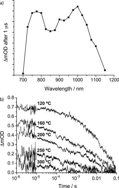
a) Transient absorption spectrum of a Sb2S3/P3HT film recorded 1 μs after photoexcitation at 650 nm. The precursor layer was annealed at 120 °C; laser excitation energy density=8.0 μJ cm−2. b) Decay in transient absorption of the P3HT hole polaron at 980 nm for Sb2S3/P3HT films as a function of annealing temperature. Laser excitation at 650 nm (8.7 μJ cm−2). Signals are scaled to account for small differences in the number of photons absorbed at 650 nm.
Our results show that long-lived separation of photogenerated charges in the Sb2S3 layer can be achieved by hole transfer to P3HT, highlighting its potential for applications in light-conversion technologies. However, in order for the mesoporous Sb2S3 structures to assume both the optical and electrical roles of a sensitized wide-band-gap metal oxide film, it is also necessary that they conduct electrons. To investigate this, we have fabricated preliminary photovoltaic devices using an architecture borrowed from the blended inorganic–organic hybrid system (glass/ITO/TiO2 (dense)/CdS/Sb2S3/P3HT/PEDOT:PSS/Ag).[4b,d] In these cells, photogenerated electrons and holes are collected at the ITO and Ag electrodes, respectively. Full details of the device-fabrication procedure are given in the Supporting Information. Figure 4 a shows the current–voltage trace for a typical device under one sun equivalent of illumination with an overall power conversion efficiency (PCE) of 0.94 %. Importantly, although the low fill factor of 36.2 % suggests a suboptimal device architecture, a short-circuit current of 4.6 mA cm−2 is achieved, which shows that the Sb2S3 layer is indeed able to conduct photogenerated charge. We expect that significant improvements in device performance will be achieved by tailoring the device architecture specifically to this system, for example through the optimization of charge-selective interlayers and contacts. Figure 4 b shows a typical IPCE spectrum, with the generation of photocurrent beyond 700 nm highlighting the contribution of photoinduced hole transfer from Sb2S3 to P3HT. A lack of photocurrent contribution from P3HT is reflected by depression of the IPCE where the polymer absorbs (ca. 500–640 nm), which is consistent with our transient absorption measurements and reports in the literature of TiO2/Sb2S3/P3HT systems.[8b] This issue can be addressed by the use of either transparent or near-infrared-absorbing polymers, as well as by further tuning the system morphology.
Figure 4.
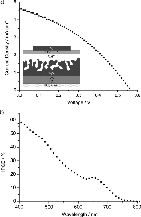
a) Current–voltage response of an ITO/TiO2/CdS/Sb2S3/P3HT/PEDOT:PSS/Ag photovoltaic device under one sun equivalent of illumination; the inset shows the device architecture. b) Incident photon-to-current efficiency of an ITO/TiO2/CdS/Sb2S3/P3HT/PEDOT:PSS/Ag device.
In conclusion, we have demonstrated a facile, low-temperature processing route to mesostructured Sb2S3 films, in which porosity and morphology can be controlled through variation of the annealing temperature. The resultant films are highly photosensitive, with an absorption edge of approximately 740 nm. When the pores of the Sb2S3 layers are filled with a polymer, photoinduced separation of charges occurs across the inorganic/organic heterojunction, as demonstrated by transient absorption spectroscopy. The fabrication of functioning photovoltaic devices with short-circuit currents approaching 5 mA cm−2 confirms that the Sb2S3 layer is electrically, as well as optically active. While this method has been applied to the decomposition of antimony xanthates, we expect it to be equally applicable to other metal–xanthate precursors, providing a general platform for the growth of colored, electrically connected mesoporous films of inorganic semiconductors.
Supporting Information
As a service to our authors and readers, this journal provides supporting information supplied by the authors. Such materials are peer reviewed and may be re-organized for online delivery, but are not copy-edited or typeset. Technical support issues arising from supporting information (other than missing files) should be addressed to the authors.
miscellaneous_information
References
- 1a.O’Regan BC, Grätzel M. Nature. 1991;353:737–740. [Google Scholar]
- 1b.Tilley SD, Cornuz M, Sivula K, Grätzel M. Angew. Chem. 2010;122:6549–6552. doi: 10.1002/anie.201003110. [DOI] [PubMed] [Google Scholar]
- Angew. Chem. Int. Ed. 2010;49:6405–6408. doi: 10.1002/anie.201003110. [DOI] [PubMed] [Google Scholar]
- 2a.Hagfeldt A, Boschloo G, Sun L, Kloo L, Pettersson H. Chem. Rev. 2010;110:6595–6663. doi: 10.1021/cr900356p. [DOI] [PubMed] [Google Scholar]
- 2b.Hodes G, Cahen D. Acc. Chem. Res. 2012;45:705–713. doi: 10.1021/ar200219h. [DOI] [PubMed] [Google Scholar]
- 2c.Robertson N. Angew. Chem. 2006;118:2398–2405. [Google Scholar]
- Angew. Chem. Int. Ed. 2006;45:2338–2345. doi: 10.1002/anie.200503083. [DOI] [PubMed] [Google Scholar]
- 3a.Efrima S, Pradhan N. C. R. Chim. 2003;6:1035–1045. [Google Scholar]
- 3b.Malik MA, Afzaal M, O’Brien P. Chem. Rev. 2010;110:4417–4446. doi: 10.1021/cr900406f. [DOI] [PubMed] [Google Scholar]
- 4a.Leventis HC, King SP, Sudlow A, Hill MS, Molloy KC, Haque SA. Nano Lett. 2010;10:1253–1258. doi: 10.1021/nl903787j. [DOI] [PubMed] [Google Scholar]
- 4b.Dowland S, Lutz T, Ward A, King SP, Sudlow A, Hill MS, Molloy KC, Haque SA. Adv. Mater. 2011;23:2739–2744. doi: 10.1002/adma.201100625. [DOI] [PubMed] [Google Scholar]
- 4c.Rath T, Edler M, Haas W, Fischereder A, Moscher S, Schenk A, Trattnig R, Sezen M, Mauthner G, Pein A, Meischler D, Bartl K, Saf R, Bansal N, Haque SA, Hofer F, List EJW, Trimmel G. Adv. Energy Mater. 2011;1:1046–1050. [Google Scholar]
- 4d.Bansal N, O’Mahony FTF, Lutz T, Haque SA. Adv. Energy Mater. 2013;3:986–990. [Google Scholar]
- 4e.Reynolds LX, Lutz T, Dowland S, MacLachlan A, King S, Haque SA. Nanoscale. 2012;4:1561–1564. doi: 10.1039/c2nr12081j. [DOI] [PubMed] [Google Scholar]
- 5.Lutz T, MacLachlan A, Sudlow A, Nelson J, Hill MS, Molloy KC, Haque SA. Phys. Chem. Chem. Phys. 2012;14:16192–16196. doi: 10.1039/c2cp43534a. [DOI] [PubMed] [Google Scholar]
- 6.Versavel M, Haber J. Thin Solid Films. 2007;515:7171–7176. [Google Scholar]
- 7a.Savadogo O. J. Electrochem. Soc. 1992;139:L16–L16. [Google Scholar]
- 7b.Savadogo O, Mandal KC. Appl. Phys. Lett. 1993;63:228–228. [Google Scholar]
- 8a.Itzhaik Y, Niitsoo O, Page M, Hodes G. J. Phys. Chem. C. 2009;113:4254–4256. [Google Scholar]
- 8b.Chang JA, Im SH, Lee YH, Kim H-J, Lim C-S, Heo JH, Seok SI. Nano Lett. 2012;12:1863–1867. doi: 10.1021/nl204224v. [DOI] [PubMed] [Google Scholar]
- 8c.Ito S, Tsujimoto K, Nguyen D-C, Manabe K, Nishino H. Int. J. Hydrogen Energy. 2013 DOI 10.1016/j.ijhydene.2013.02.069. [Google Scholar]
- 9.O’Mahony FTF, Lutz T, Guijarro N, Gómez R, Haque SA. Energy Environ. Sci. 2012;5:9760–9760. [Google Scholar]
- 10.Pradhan N, Katz B, Efrima S. J. Phys. Chem. B. 2003;107:13843–13854. [Google Scholar]
- 11.Bansal N, Reynolds LX, MacLachlan A, Lutz T, Ashraf RS, Zhang W, Nielsen CB, McCulloch I, Rebois DG, Kirchartz T, Hill MS, Molloy KC, Nelson J, Haque SA. Sci. Rep. 2013;3:1531. doi: 10.1038/srep01531. [DOI] [PMC free article] [PubMed] [Google Scholar]
Associated Data
This section collects any data citations, data availability statements, or supplementary materials included in this article.
Supplementary Materials
miscellaneous_information


