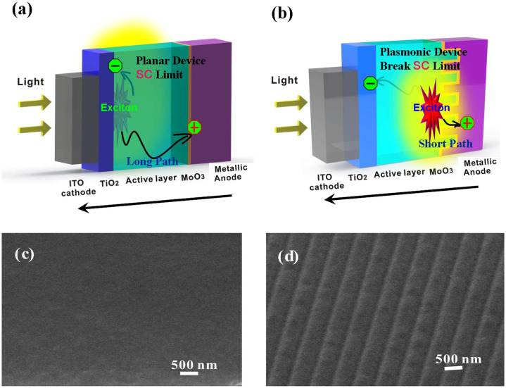
Figure 1. A schematic pattern of inverted OSC devices.
(a) inverted OSCs with a planar metallic anode; (b) inverted OSCs with a grating metallic anode. The device structure of the planar-inverted OSC is: ITO (70 nm)/TiO2 (20 nm)/P3HT:PCBM (220 nm)/MoO3 (10 nm)/planar Ag or Au (100 nm); and the device structure of the grating-inverted OSC is: ITO (70 nm)/TiO2 (20 nm)/P3HT:PCBM grating (220 nm)/MoO3 (10 nm)/Ag or Au grating (100 nm). The short notation “SC” denotes the space charge. A long transport path of holes in the planar-inverted OSC induces the SCL characteristics. A short transport path of holes manipulated by the plasmonic-electrical effect in the grating-inverted OSC breaks the SCL. (c) 45°-tilt SEM image of the planar P3HT:PCBM film. (d) 45°-tilt SEM image of the P3HT:PCBM film with the grating structure.

