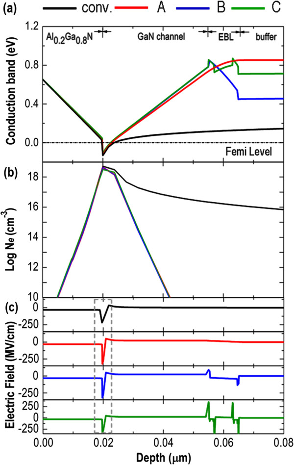
Figure 2.

Conduction band, electron density, and electric field distribution versus depth plots. (a) Calculated conduction band profiles of all devices under the neutral bias condition. (b) Distribution of three-dimensional electron density (Ne) in a semi-log scale for all devices. (c) Corresponding electric field distributed over all devices. The dotted-line rectangle marks the region where the 2-DEG channel belongs.
