Figure 4.
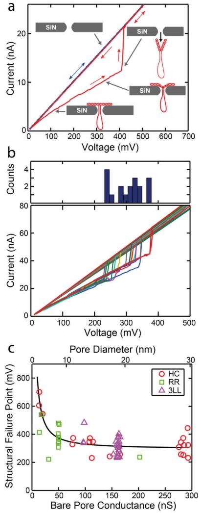
a) IV curve (red) showing a 2LL nanoplate undergoing structural failure and being pulled through a 9 nm pore. Once pulled through, the conductance of the pore returns to the level seen for the bare pore (blue dots). b) IV curves of 18 different 3LL nanoplates being pulled through a 19 nm pore. Top panel displays a histogram of the structural failure points. c) The structural failure points for three nanoplate designs docked onto different-diameter pores. It can be seen that smaller pores require a greater force to pull the nanoplate through. The solid line has been added to guide the eyes.

