Abstract
We have developed two techniques for time-resolved x-ray diffraction from bulk polycrystalline materials during dynamic loading. In the first technique, we synchronize a fast detector with loading of samples at strain rates of ∼103–104 s−1 in a compression Kolsky bar (split Hopkinson pressure bar) apparatus to obtain in situ diffraction patterns with exposures as short as 70 ns. This approach employs moderate x-ray energies (10–20 keV) and is well suited to weakly absorbing materials such as magnesium alloys. The second technique is useful for more strongly absorbing materials, and uses high-energy x-rays (86 keV) and a fast shutter synchronized with the Kolsky bar to produce short (∼40 μs) pulses timed with the arrival of the strain pulse at the specimen, recording the diffraction pattern on a large-format amorphous silicon detector. For both techniques we present sample data demonstrating the ability of these techniques to characterize elastic strains and polycrystalline texture as a function of time during high-rate deformation.
I. INTRODUCTION
The response of materials to high-strain-rate mechanical deformation is of interest in many fields including the automotive, aerospace, and defense industries.1 The compression Kolsky bar2–7 (also called the split Hopkinson pressure bar) is commonly used to study the stress-strain behavior of materials over strain rates of ∼103–105 s−1. Information about structural evolution in these experiments is usually inferred from the starting and ending microstructures, or by performing recovery experiments at various levels of strain. However, post-mortem microstructures may be different from the non-equilibrated structures present during the dynamic event.
Time-resolved x-ray diffraction can provide important insights into the evolution of the structure of a material during dynamic loading, such as the elastic strains in individual phases, crystallographic texture, and the development of new (possibly metastable) phases. Earlier work demonstrated the utility of x-ray diffraction studies of single crystals under shock loading.8–13 In this paper, we describe two techniques for obtaining structural information via x-ray diffraction from polycrystalline materials during dynamic deformation at strain rates of ∼103 s−1. Diffraction provides complementary information to imaging, which has previously been used to track damage evolution at similar strain rates.14
Our two techniques take different approaches to achieving the microsecond-scale temporal resolution necessary for in situ studies during dynamic loading in a Kolsky bar test, which has a typical duration of ∼100 μs for studies of ductile metals. The most straightforward approach is to use an x-ray detector capable of recording multiple frames with integration times on the microsecond scale, such as the Keck pixel array detector (PAD) developed at Cornell University.15 The x-ray absorption in the silicon detection layer used in this PAD is directly related to the x-ray sensitivity of the detector, which falls quickly for x-ray energies above 25 keV. High energies are desirable, however, for studies of strongly absorbing materials and for bulk specimens (∼mm thickness) in general. For such cases, we use a different approach to temporal resolution in which we produce a short pulse of x-rays using a high-speed shutter and record the diffraction pattern onto a detector slower than the Keck PAD but with better sensitivity to high-energy x-rays. In this case, we can only record one diffraction pattern per experiment and must build up a picture of the evolution of the structure during loading from separate experiments on multiple, nominally identical specimens.
II. FAST DETECTOR TECHNIQUE
A. Experimental setup
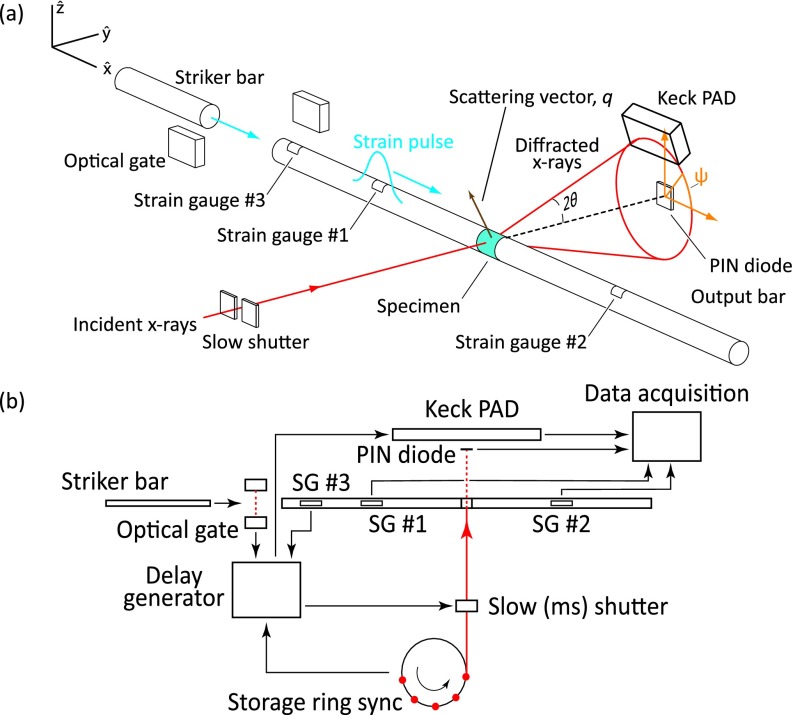
Figure 1(a) shows a schematic of the experiment in which we used a fast Keck PAD for temporal resolution. We conducted these experiments in hutch G3 at the Cornell High Energy Synchrotron Source (CHESS) using a 1 mm × 1 mm beam of 10 keV x-rays. We used a multilayer monochromator which produced a relatively broad bandpass beam (ΔE/E ≃ 2%) with a flux of approximately 2 × 10¹³ ph s−1 mm−2.
FIG. 1.
(a) Experimental setup used for fast detector experiments, showing scattering in a vertical plane and the scattering vector transverse to the loading axis. Strain gauges 1 and 2 were used to extract stress-strain data; strain gauge 3 was used to trigger the PAD. (b) Timing signals for the fast detector experiments.
We positioned a Kolsky bar (with 3 mm diameter aluminum bars) in the incident beam. For most of our experiments, the incident beam was normal to the bar and the detector rotated in a vertical plane about the loading axis (i.e., the x axis in Figure 1), so that the scattering plane was vertical and the scattering vector perpendicular to the loading direction. In this geometry the structural information comes from scattering planes parallel to the loading direction. For some experiments we rotated the bar and detector about a vertical axis (the z axis in Figure 1(a)), making the scattering plane horizontal and choosing the incident and scattering angles so that the scattering vector was parallel to the loading direction; in this geometry the scattering planes were perpendicular to the loading direction.
The samples tested in these experiments were magnesium alloy AZ31 with a typical grain size of 3 μm produced by equal-channel angular extrusion. We cut samples from the extruded ingots by electric discharge machining (EDM) and mechanically polished them into ∼0.6 × 1 × 1.5 mm right rectangular prisms with loading surfaces polished to a finish of 5 μm. Samples were loaded along the 1.5 mm direction and x-rays were transmitted through the 0.6 mm direction to minimize clipping of the x-ray beam by the bars and to maximize x-ray transmission, respectively.
B. Detector and timing
The detector used for these experiments was based on analog pixel array detector chips with a minimum integration time of 150 ns or less.15 Each chip consists of a 128 × 128 array of 150 μm pixels. We assembled a 2 × 3 array of individual PAD chips to produce a detector with a total area of 57.6 × 38.4 mm, which covered an azimuthal angle range of ∼48° in our experimental setup. The PAD can store eight frames before readout, so it was necessary to trigger the detector at an appropriate time relative to the arrival of the strain pulse at the specimen. We did this by placing a semiconductor strain gage (strain gauge 3 in Fig. 1) near the end of the input bar close to the projectile; the rise in signal from this strain gage triggered a delay generator which in turn triggered the Keck PAD via a transistor-transistor logic (TTL) pulse after a suitable delay (based on the speed of sound in the incident bar and the distance from strain gage to specimen). By appropriate choices of delay time, integration time, and time between frames we were able to capture diffraction patterns during the entire course of deformation or during any portion of interest. In various experiments we used integration times ranging from the shortest possible with this detector (150 ns) to approximately 10 μs.
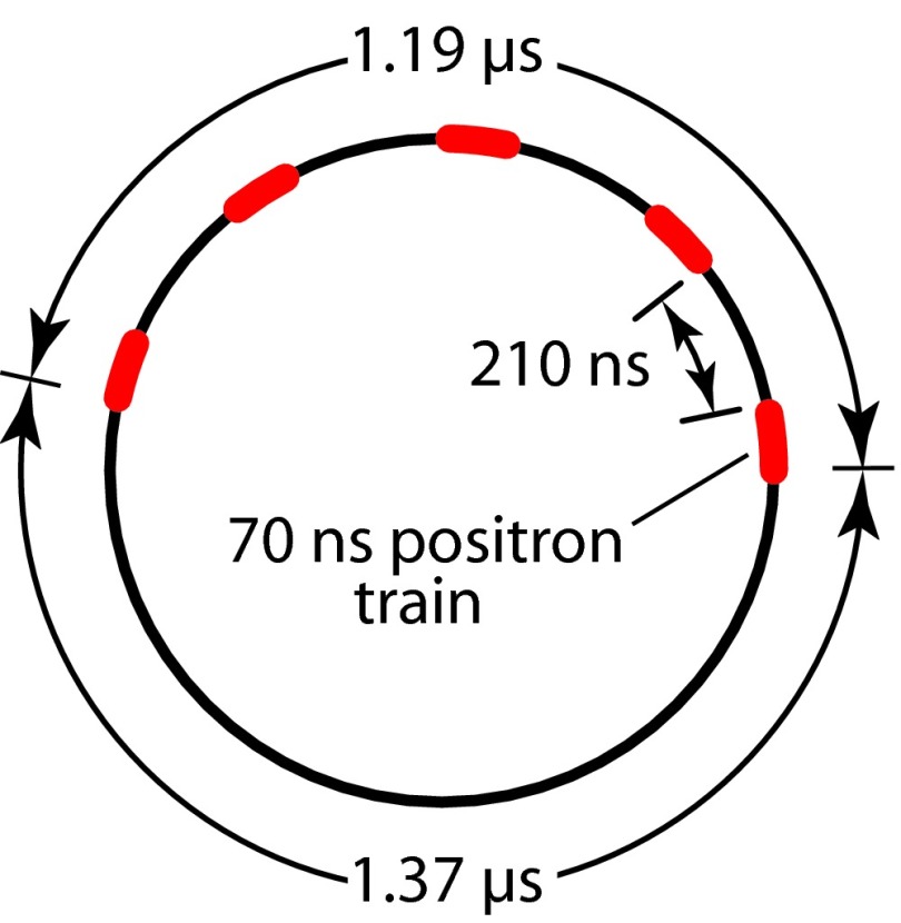
Timing experiments on the microsecond scale require attention to the pulsed nature of synchrotron radiation. During these experiments the positron bunch structure in the Cornell Electron Storage Ring (CESR) consisted of five trains of bunches with each train having a duration of 70 ns. The five trains were equally spaced over a span of 1.19 μs followed by a 1.37 μs gap, for a ring period of 2.56 μs (Fig. 2). Under these conditions the x-ray exposure during the time the detector is counting can vary depending on when the integration time starts relative to the position of the bunches in the ring. For example, a 1 μs integration might occur during the 1.37 μs gap, when there are no x-rays incident on the specimen. To avoid this we implemented an additional delay that inhibited the detector from triggering until it received a timing signal indicating the arrival of the first bunch in the next ring period (Fig. 1(b)). Because we had no way to time the arrival of the strain pulse at the specimen relative to the positions of the positron bunches this introduced a jitter in the timing of the first diffraction pattern of up to 2.56 μs (corresponding to the worst-case scenario where the detector has to wait a full ring period before beginning counting). We also arranged the timing so that each frame after the first occurred an integral number of ring periods after the preceding frame. In this way we were able to ensure consistent x-ray exposures for each frame.
FIG. 2.
The bunch structure for the fast detector experiments consisted of five 70 ns positron trains separated by 210 ns, with an overall ring period of 2.56 μs.
C. Sample data
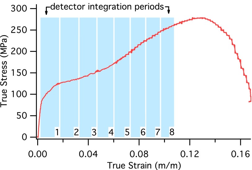
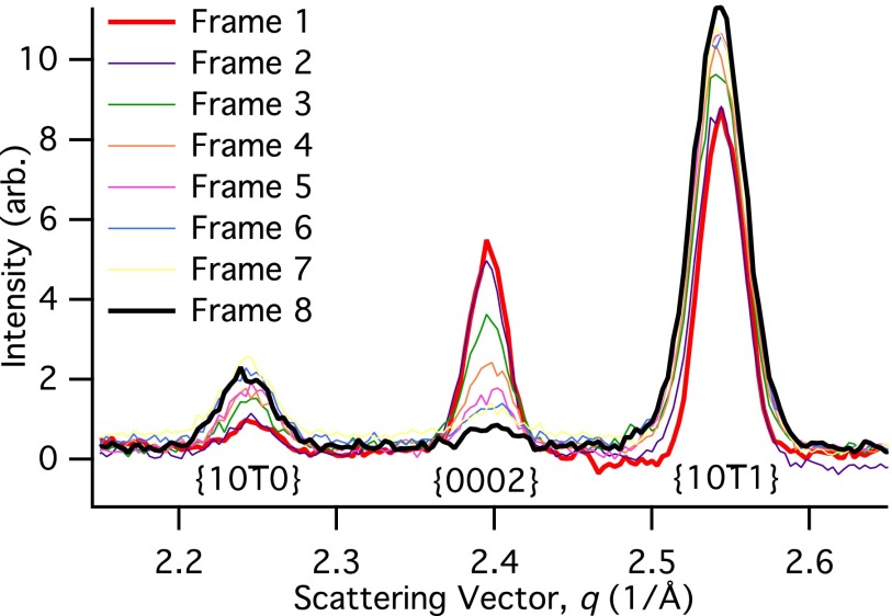
Figure 3 shows a stress-strain curve obtained at CHESS along with the times over which each diffraction pattern was collected. The exposure time for these patterns was 3.75 μs, corresponding to two 2.56 μs ring periods minus the trailing 1.37 μs gap. After background subtraction, we azimuthally integrated the powder diffraction data from the Keck PAD to produce plots of scattered intensity vs. scattering vector magnitude q = 4πsin θ/λ, as shown in Fig. 4 for data collected with transverse to the loading direction. The , {0002}, and peaks from Mg are clearly defined, and we are able to track changes in peak position and peak area for all three. In particular the decrease in intensity of the {0002} peak intensity coupled with the increase in the peak is suggestive of deformation by twinning of magnesium.16
FIG. 3.
True stress-true strain curve of AZ31 magnesium alloy overlayed with Keck PAD signal indicating the start of data collection by the x-ray detector.
FIG. 4.
Plots of integrated intensity vs. scattering vector for the , {0002}, and planes of AZ31 corresponding to the stress-strain curve in Figure 3, with exposure times of 3.75 μs.
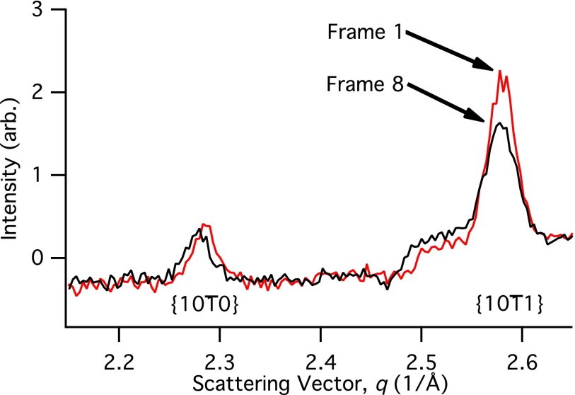
Figure 5 shows examples of data collected with the shortest exposure attempted, a 150 ns integration time synchronized to coincide with a single 70 ns positron bunch train (Fig. 2). As expected, the signal-to-noise ratio is poorer than for the longer exposures in Fig. 4, but, due to the pulsed synchrotron source, the x-ray intensity only drops by a factor of 10 between the two data sets while the temporal resolution is increased by a factor of 50. The and diffraction peaks are still clearly discernible and changes in the peak area are apparent. The absence of the {0002} peak is probably due to the initial crystallographic texture of the specific specimen being tested.
FIG. 5.
Example data collected with experimental parameters similar to those used in Figure 4 but with exposure times of 70 ns.
III. CONSIDERATIONS IN EXPERIMENTAL DESIGN
When designing in situ diffraction experiments it is useful to be able to estimate the expected signal given the experimental configuration and samples to be studied. This can guide the selection of the x-ray energy or other experimental parameters, and even help one decide whether a contemplated experiment is feasible. For powder x-ray diffraction experiments one important and easily calculated quantity is the integrated intensity from the {hkl} planes,
| (1) |
where Φ is the incident beam flux (ph s−1mm−2), r0 is the classical radius of an electron (2.82 × 10⁻¹⁵ m), P is the polarization factor (≃1 for scattering in the vertical plane at a synchrotron), As is the absorption factor for the sample (discussed below), Fhkl is the structure factor, λ is the x-ray wavelength, vuc is the volume of the unit cell, mhkl is the multiplicity of the {hkl} planes, L is the sample-to-detector distance, θ is one-half of the scattering angle, (1 − Ad) is the efficiency of the detector (discussed below), Aair is the absorption factor for x-rays in air (from the sample to detector, for instance), Δx is the size of a pixel on the detector, and Δt is the integration time. Note that I represents the intensity of the peak integrated along (transverse to a powder ring, analogous to integrating over 2θ for a conventional diffraction pattern) while Δx is the pixel size in the transverse direction (i.e., around a ring).
For our experimental geometry in which the incident beam is normal to the sides of a flat planparallel specimen the absorption factor is17
| (2) |
where Abeam is the cross-sectional area of the incident x-ray beam, t is the specimen thickness, and μ is the linear absorption coefficient of the specimen.
The two parameters in Eqs. (1) and (2) most directly under the control of the experimenter are the x-ray wavelength and the sample thickness. It is easily shown17 that the optimal thickness of a sample for a transmission diffraction experiment is 1/μ. For in situ loading experiments the optimal thickness must be balanced against the needs of the loading apparatus; in the case of Kolsky-type experiments samples with thickness ∼1 mm for a length along the compression direction of ∼0.6 mm (to maintain an aspect ratio l/d ∼0.5–1) are fairly routine. Thinner samples are possible but pose increasing difficulties, with a practical limit of about 0.5 mm for routine experiments.
For the magnesium specimens discussed above and 10 keV x-rays, 1/μ = 0.28 mm so our 0.6 mm specimens were thicker than would be optimal for the x-ray experiments, but this less-than-ideal thickness kept the specimens at an acceptable aspect ratio for the Kolsky bar experiments. Magnesium is among the lightest metals, though, and it is clear that studies of heavier elements would be infeasible at this x-ray energy. The obvious solution is to select a higher x-ray energy, but the efficiency of the Keck PAD drops due to decreasing absorption in the detection layer. To a reasonable approximation we can assume that any photon absorbed in the Si detection layer is detected, so the efficiency of the detector is
| (3) |
where μSi is the linear absorption coefficient for Si and tSi = 500 μm is the thickness of the detection layer. A complete description of the efficiency of the experiment needs to incorporate this factor into Eq. (1). The drop in detector efficiency at high x-ray energies means that a different approach is required to study materials with higher atomic number that are strongly absorbing.
IV. FAST SHUTTER TECHNIQUE
For the reasons just discussed, higher x-ray energies are required when studying transition metals and other strongly absorbing materials. Due to the low efficiency of the present Keck PAD at energies above 25 keV we employed an alternative technique in which we achieved temporal resolution on the microsecond scale by producing short x-ray pulses. A similar pulsed technique has been used by us and others for studies of irreversible transformations in materials.18–20
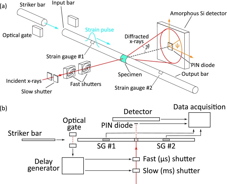
We conducted these experiments at beamline 1-ID of the Advanced Photon Source (APS) using a monochromatic 86 keV x-ray beam vertically focused to a spot size of ∼30 μm × 1 mm together with a large-format amorphous silicon detector centered on the transmitted beam (Fig. 6(a)). Both the bandpass (∼0.01%) and the flux (∼1012 ph s−1 mm−2) of this beam were smaller than that at CHESS. The amorphous silicon detector is too slow (30 Hz) to capture multiple diffraction patterns during a single test, so to track the evolution of structure during deformation we performed separate tests on multiple, nominally identical specimens with different shutter delays to interrogate different times during the loading. The samples for these experiments were Monel®-400 (Cu-Ni) fabricated by EDM into 3 × 3 × 4 mm (l/d ∼ 1.3) rectangular prisms with loading surfaces polished to a 3 μm finish. We used a larger Kolsky bar apparatus for these specimens, with 8 mm diameter maraging steel bars.
FIG. 6.
Schematic (a) and timing signals (b) for the fast detector experiments.
A. Timing
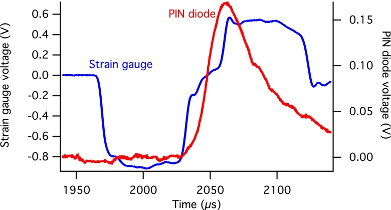
To produce short x-ray pulses we positioned a fast shutter system18 in the incident beam upstream of the specimen. The pulses produced using this system had a full-width at half maximum of approximately 40 μs (Fig. 7) as measured by a p-type, intrinsic, n-type semiconductor (PIN) diode mounted on the beam stop in the transmitted beam. In previous experiments with smaller x-ray beams and lower x-ray energies the same shutters produced pulses of <20 μs (Ref. 18); the longer pulses here are due to a combination of a larger beam (requiring more time to occlude) and higher energy (which reduces the stopping power of the tungsten blades). Even with pulses of this length we are able to clearly observe the evolution of the structure, as described below.
FIG. 7.
An example of the signal detected on the PIN diode (indicative of the number of photons passing through the specimen) as a function of time, superimposed with the incident bar strain gauge signal that was obtained simultaneously.
In the pulsed experiments the critical timing event is the arrival of the strain pulse at the specimen, which must be synchronized with the timing of the x-ray pulse (Fig. 6(b)). In principle we could trigger the shutters from a strain gage signal on the incident bar, but in practice the time required to actuate the shutters (∼350 μs) exceeds the time for the strain pulse to propagate down the input bar. Instead, we triggered the shutters off of an optical gate positioned to sense the arrival of the striker bar at the input bar (Fig. 6). A similar method, using a piezoelectric pin rather than an optical gate, has previously been used for timing high-speed phase contrast imaging and diffraction during dynamic loading.12,13
Variations in velocity of the striker bar, due mostly to variations in breech pressure between shots, make this approach less reproducible than triggering off of the strain pulse as was done in the fast detector experiments described above. In our trials the measured variation in striker velocity was approximately 10%, which created an uncertainty in timing the x-ray pulse relative to the arrival of the strain pulse at the specimen of up to 220 μs. In future experiments this may be reduced either by using a piezoelectric pin12,13 or possibly by using two optical gates to measure the velocity of the striker bar and adjust the shutter trigger delay accordingly.
For these experiments the APS storage ring was operating in its standard 24 bunch mode with 153 ns between bunches. With 40 μs exposures, each diffraction pattern therefore integrates over hundreds of bunches. Improved temporal resolution would be possible with the higher flux of a broad bandpass beam, including the possibility of synchronization to single bunches in the APS hybrid fill mode. This would require either an improved shutter or a high-speed beam chopper, or a gated detector.
B. Sample data
One advantage of the large size of the detector coupled with the high x-ray energies (which compress the scattering into smaller angles 2θ) was that we could observe complete diffraction rings associated with {111}, {200}, and {220} reflections in the specimens. We calculated the strain using the method of Wanner and Dunand.21 In this method the ring diameter is determined as a function of azimuthal angle ψ by dividing the ring into a number of evenly spaced bins (60 in our case) and using diametrically opposed bins to minimize errors associated with uncertainty in the beam position. Due to elastic strain the diffraction ring is elliptical, so the ring diameter is approximated as D(ψ) = a + (b − a)sin 2 ψ where a and b are constants determined by fitting this expression to the measured D(ψ). The semiaxes of the ring are found using a and b to calculate the ring diameter at ψ = 0° (the loading direction) and at ψ = 90° (the transverse direction). With the semiaxes in the strained state known the elastic strain in the loading and transverse directions can be calculated using the ring diameter of the unstrained specimen.21,22
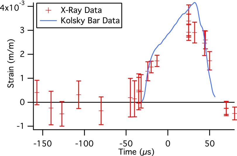
A plot of the elastic strain in the loading direction as a function of time for {111} planes is shown in Fig. 8. Using the point of maximum intensity from the PIN diode signal and the signal recorded by the strain gauges (Fig. 7), each diffraction pattern could be assigned a time point relative to the onset of deformation. We note, however, that each data point actually represents an integration over a longer period of time. Also shown in Fig. 8 is the lattice strain as a function of time for {111} planes with their normals along the loading direction, calculated from the global average stress (from the Kolsky bar strain gage data) using the diffraction elastic constants for Monel®-400 (Ref. 23). The measured strain agrees reasonably well with the calculation, allowing for the fact that the diffraction patterns average over a longer interval of time (during parts of which the sample sees lower load).
FIG. 8.
Measured elastic strain in the loading direction as a function of time for {111} planes in the Monel®-400 specimens, superimposed with predicted strain in the loading direction for grains with their {111} plane normals aligned along the loading direction, from the Kolsky bar stress-strain data and the Kröner elasticity model.23
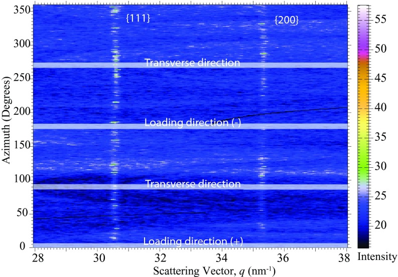
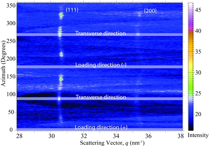
Figure 9 shows an intensity map of the {111} and {200} powder rings as a function of scattering vector magnitude q and azimuthal angle ψ made using a 40 μs exposure taken ∼107 μs before the onset of deformation.24 Figure 10 shows an intensity map of these same rings with an exposure of the same duration taken ∼32 μs after the onset of deformation. In the undeformed specimens the {111} and {200} rings are continuous and have nearly uniform intensity, indicative of a material that has little crystallographic texture. During dynamic loading crystallographic texture clearly develops, which appears most obviously as an increase in the intensity of the {111} ring near ψ = ±45°, ±90°, and ±135°. A similar but less pronounced variation in the {200} ring intensity can also be observed.
FIG. 9.
Intensity map as a function of scattering vector and azimuthal angle on the detector for the {111} and {200} planes of Monel®-400, made using a 40 μs exposure taken 107 μs before the onset of deformation in the specimen.
FIG. 10.
Intensity map as a function of scattering vector and azimuthal angle on the detector for the {111} and {200} planes of Monel®-400, made using a 40 μs exposure taken 32 μs after the onset of deformation in the specimen.
V. CONCLUSIONS
The results shown here demonstrate the ability to perform transmission x-ray diffraction on bulk metallic specimens during dynamic loading with microsecond-scale temporal resolution. This allows for the observation of irreversible dynamic microstructural evolution, including the evolution of lattice strains and texture. In principle it also allows for the observation of stress- or strain-induced phase transformations during high-strain-rate loading, including the appearance of transient phases.
The techniques we have demonstrated here offer both advantages and disadvantages for characterizing materials. The fast PAD technique provides excellent temporal resolution and reliable timing and permits observation of the structural evolution of individual specimens. However, the existing Keck PAD is relatively small (limiting the range of q space that can be covered) and has poor sensitivity for high-energy x-rays that are necessary to study strongly absorbing materials such as transition metals. The fast shutter technique permits the use of high x-ray energies to study such specimens, but at the expense of less reliable timing and the ability to produce only one diffraction pattern per test. We anticipate that future developments in detector technology will permit the use of fast high-energy x-ray detectors, overcoming many of these limitations. Specifically, the Cornell participants are exploring larger arrays of Keck PADs utilizing sensor materials with higher atomic number for greater efficiency at high x-ray energy.
Although to date we have only performed experiments on samples loaded in uniaxial compression, the Kolsky bar technique has the flexibility to provide other loading conditions such as tension, compression/shear, and pure shear.25–27 We expect, therefore, that the techniques described here can readily be adapted to a wide range of loading conditions. It should also be possible to combine in situ diffraction with in situ radiography and/or phase contrast imaging (as has previously been done in the context of rapid phase transformations28). With a polychromatic x-ray beam it should be possible to examine single crystals under dynamic loading, and one might even imagine small-angle x-ray scattering (SAXS) studies of damage evolution.
ACKNOWLEDGMENTS
The authors would like to acknowledge A. Mashayekhi, L. Zhou, and K. Goetze for their contributions to this work. This work was sponsored in part by the Army Research Laboratory and was accomplished under Cooperative Agreement No. W911NF-12-2-0022. The views and conclusions contained in this document are those of the authors and should not be interpreted as representing the official policies, either expressed or implied, of the Army Research Laboratory or the U.S. Government. The U.S. Government is authorized to reproduce and distribute reprints for government purposes notwithstanding any copyright notation herein. Financial support for this work was also provided by the US Navy under the MURI Program (Grant ONR MURI N00014-61007-1-0740). Use of the Advanced Photon Source, an Office of Science User Facility operated for the U.S. Department of Energy (DOE) Office of Science by Argonne National Laboratory, was supported by the U.S. DOE under Contract No. DE-AC02-06CH11357. P.K.L. would like to acknowledge OSD-T&E (Office of Secretary Defense-Test and Evaluation), Defense-Wide/PE0601120D8Z National Defense Education Program (NDEP)/BA-1, Basic Research, for their support. Detector development at Cornell is supported by the DOE Grant No. DE-FG02-10ER46693, the Keck Foundation, and CHESS. CHESS is supported by the NSF and NIH-NIGMS under NSF Grant No. DMR-0936384.
REFERENCES
- 1.Meyers M., Dynamic Behavior of Materials (John Wiley and Sons, New York, 1994). [Google Scholar]
- 2.Kolsky H., Proc. Phys. Soc. B 62, 676 (1949). 10.1088/0370-1301/62/11/302 [DOI] [PubMed] [Google Scholar]
- 3.Chen W. and Song B., Split Hopkinson (Kolsky) Bar: Design, Testing, and Applications (Springer, New York, 2011). [Google Scholar]
- 4.Chen W. and Ravichandran G., J. Mech. Phys. Solids 45(8), 1303 (1997). 10.1016/S0022-5096(97)00006-9 [DOI] [Google Scholar]
- 5.Chichili D., Ramesh K., and Hemker K., Acta Mater. 46(3), 1025 (1998). 10.1016/S1359-6454(97)00287-5 [DOI] [Google Scholar]
- 6.Johnson T. P. M., Sarva S. S., and Socrate S., Exp. Mech. 50(7), 931 (2010). 10.1007/s11340-009-9305-y [DOI] [Google Scholar]
- 7.Jia D. and Ramesh K., Exp. Mech. 44(5), 445 (2004). 10.1007/BF02427955 [DOI] [Google Scholar]
- 8.Johnson Q., Mitchell A., and Evans L., Nature (London) 231, 310 (1971). 10.1038/231310b0 [DOI] [Google Scholar]
- 9.Rigg P. and Gupta Y., Appl. Phys. Lett. 73(12), 1655 (1998). 10.1063/1.122236 [DOI] [Google Scholar]
- 10.Gupta Y. M., Turneaure S. J., Perkins K., Zimmerman K., Arganbright N., Shen G., and Chow P., Rev. Sci. Instrum. 83(12), 123905 (2012). 10.1063/1.4772577 [DOI] [PubMed] [Google Scholar]
- 11.Suggit M. J., Higginbotham A., Hawreliak J. A., Mogni G., Kimminau G., Dunne P., Comley A. J., Park N., Remington B. A., and Wark J. S., Nat. Commun. 3, 1224 (2012). 10.1038/ncomms2225 [DOI] [PubMed] [Google Scholar]
- 12.Jensen B. J., Owens C. T., Ramos K. J., Yeager J. D., Saavedra R. A., Iverson A. J., Luo S. N., Fezzaa K., and Hooks D. E., Rev. Sci. Instrum. 84(1), 013904 (2013). 10.1063/1.4774389 [DOI] [PubMed] [Google Scholar]
- 13.Luo S. N., Jensen B. J., Hooks D. E., Fezzaa K., Ramos K. J., Yeager J. D., Kwiatkowski K., and Shimada T., Rev. Sci. Instrum. 83(7), 073903 (2012). 10.1063/1.4733704 [DOI] [PubMed] [Google Scholar]
- 14.Hudspeth M., Claus B., Dubelman S., Black J., Mondal A., Parab N., Funnell C., Hai F., Qi M. L., Fezzaa K., Luo S. N., and Chen W., Rev. Sci. Instrum. 84(2), 025102 (2013). 10.1063/1.4789780 [DOI] [PubMed] [Google Scholar]
- 15.Koerner L. J., Tate M. W., and Gruner S. M., IEEE Trans. Nucl. Sci. 56(5), 2835 (2009). 10.1109/TNS.2009.2028733 [DOI] [Google Scholar]
- 16.Barnett M. R., Mater. Sci. Eng. 464(1-2), 1 (2007). 10.1016/j.msea.2006.12.037 [DOI] [Google Scholar]
- 17.Klug H. and Alexander L., X-Ray Diffraction Procedures for Polycrystalline and Amorphous Materials (Wiley, New York, 1974). [Google Scholar]
- 18.Kelly S. T., Trenkle J. C., Koerner L. J., Barron S. C., Walker N., Pouliquen P. O., Tate M. W., Gruner S. M., Dufresne E. M., Weihs T. P., and Hufnagel T. C., J. Synchrotron Radiat. 18(3), 464 (2011). 10.1107/S0909049511002640 [DOI] [PMC free article] [PubMed] [Google Scholar]
- 19.Fuoss P. H., Kisker D. W., Lamelas F. J., Stephenson G. B., Imperatori P., and Brennan S., Phys. Rev. Lett. 69(19), 2791 (1992). 10.1103/PhysRevLett.69.2791 [DOI] [PubMed] [Google Scholar]
- 20.Irving T. C. and Maughan D. W., Biophys. J. 78(5), 2511 (2000). 10.1016/S0006-3495(00)76796-8 [DOI] [PMC free article] [PubMed] [Google Scholar]
- 21.Wanner A. and Dunand D. C., Metallurg. Mater. Trans. A 31A, 2949 (2000). 10.1007/BF02830344 [DOI] [Google Scholar]
- 22.Noyan I. and Cohen J., Residual Stress: Measurement by Diffraction and Interpretation (Springer-Verlag, New York, 1987). [Google Scholar]
- 23.Holden T. M., Clarke A. P., and Holt R. A., Metallurg. Mater. Trans. 28(12), 2565 (1997). 10.1007/s11661-997-0014-9 [DOI] [Google Scholar]
- 24.Hammersley A. P., Svensson S. O., Hanfland M., Fitch A. N., and Häusermann D., High Pressure Res. 14, 235 (1996). 10.1080/08957959608201408 [DOI] [Google Scholar]
- 25.Song B., Antoun B. R., and Jin H., Exp. Mech. 53(9), 1519 (2013). 10.1007/s11340-013-9721-x [DOI] [Google Scholar]
- 26.Zhao P. D., Lu F. Y., Lin Y. L., Chen R., Li J. L., and Lu L., Exp. Mech. 52(2), SI, 205 (2012). 10.1007/s11340-011-9534-8 [DOI] [Google Scholar]
- 27.Khan A. S., Kazmi R., and Farrokh B., Int. J. Plasticity 23, 931 (2007). 10.1016/j.ijplas.2006.08.006 [DOI] [Google Scholar]
- 28.Kelly S. T., Barron S. M., Dufresne E. M., Fezzaa K., Weihs T. P., and Hufnagel T. C., “Challenges in materials science and possibilities in 3D and 4D characterization techniques,” in Proceedings of the 31st Risø International Symposium on Materials Science, edited by Hansen N., Jensen D. Juul, Nielsen S. F., Poulsen H. W., and Ralph B. (Risø National Laboratory for Sustainable Energy, Technical University of Denmark, 2010), p. 289, 2010. [Google Scholar]


