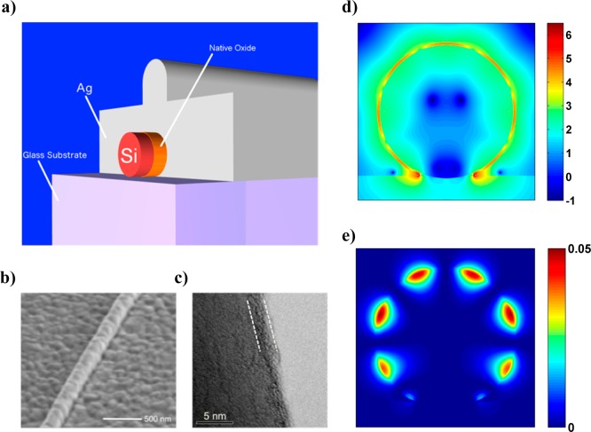
Figure 1.
(a) Schematic of silicon nanowire integrated with a 300 nm thick silver film to form a plasmonic nanocavity (drawn to scale). The native oxide of silicon (SiOx) is used to separate the active silicon core from the silver shell. (b) Scanning electron microscope (SEM) of silver-coated silicon nanowire. (c) Transmission electron microscope (TEM) image of a representative bare silicon nanowire demonstrating 1.5–2.5 nm of native oxide (denoted by dashed white lines) on the nanowire surface. (d) Frequency domain spatial distribution of the electric field intensity in Ω-cavity Si (d = 150 nm) demonstrating high order (m = 9) mode (obtained via finite difference time domain simulations) and (e) corresponding magnetic field intensity.

