Figure 3.
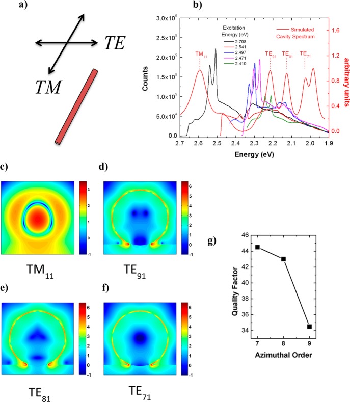
Electromagnetic mode properties of plasmonically coupled silicon analyzed via FDTD simulations and photoluminescence spectroscopy. (a) Nomenclature convention for modes polarized parallel (TM) and perpendicular (TE) to the nanowire long-axis. (b) Variable-energy excitation photoluminescence spectra of d = 150 nm Ω-cavity silicon nanowire juxtaposed with simulated cavity mode spectrum (red curve). (c–f) Frequency domain profiles of the electric intensity (log scale) for cavity modes ordered from highest to lowest energy. (h) Plot of quality factor versus azimuthal index (m), for TE modes in (b) and represented by the field profiles in (d–f).

