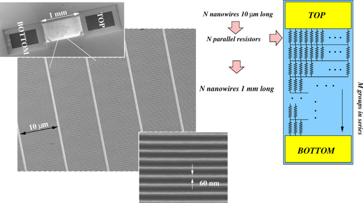
Figure 11.
Composition of SEM images of a large area network with a different texture, with respect to Figure 10. An huge number of nanowires, 10 μm long and 60 nm wide, are placed in series and in parallel. The top right sketch shows a resistor network, that represents the silicon nanowire network both from the electrical and from the thermal point of view. Reproduced with permission from ref.[101], Copyright 2013 American Chemical Society.

