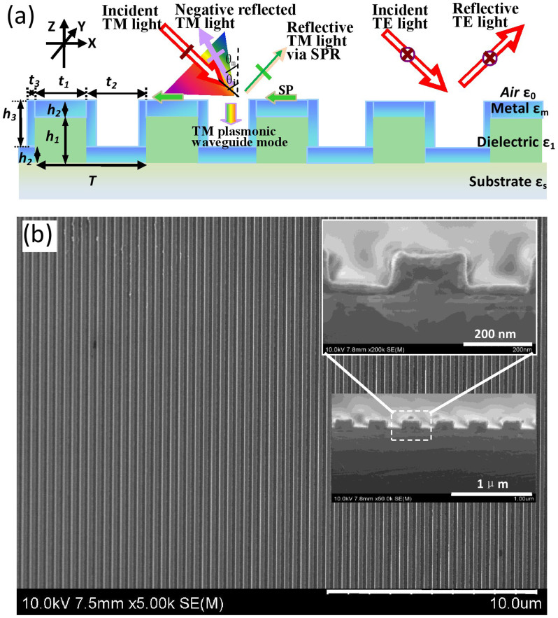
Figure 1. Structure of the metasurface beam splitter.
(a) Schematic diagram. TM light enters the slits in plasmonic waveguide mode and is reflected by the bottom Al layer. The light is strongly negatively reflected, as indicated by the chromatic sector. The reflection includes light corresponding to lateral SPR, as shown by green arrow, and light in the non-diffraction zone shown in Fig. 2(b1) and Fig. 3(b1). TE light cannot enter the slits and is primarily reflected. (b) SEM images of the top and side views (insets) of the fabricated device. The grating pitch is T = 420 nm, the width of the dielectric PMMA is t1 = 170 nm, and the width of the metal Al in the bottom PMMA-Al grating layer is t2 = 250 nm. The thicknesses of the PMMA and Al are h1 = 110 nm and h2 = 30 nm, respectively. The size of the Al on the sidewalls of the PMMA grating lines is t3 × h3 = 20 nm × 110 nm. The substrate is silicon.

