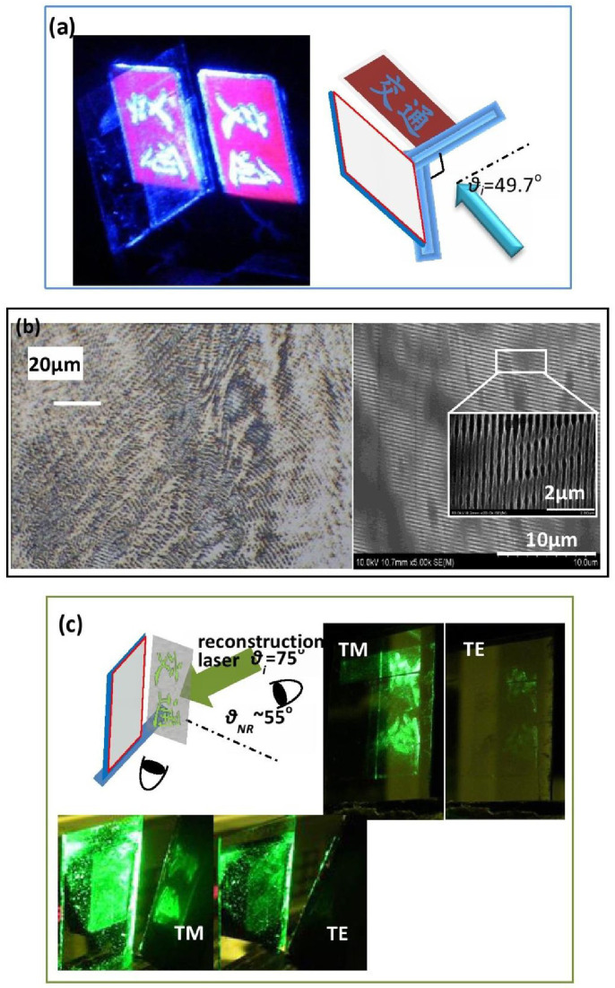
Figure 7. Metasurface hologram.
(a) Photoresist hologram fabrication scheme: The badge was placed perpendicularly to the photoresist film, and both were illuminated by a large cross-section collimated laser beam with an incident angle of 49° to the photoresist film. (b) Microscopy and SEM images of the top views of the metasurface hologram film at different scales. The film consists of randomly distributed B-MNGs with a pitch of 300 nm. The width of the dielectric PMMA is t1 = 150 nm, and the thicknesses of the PMMA and Al are h1 = 110 nm and h2 = 50 nm, respectively. (c) Real images reconstructed using TM and TE laser light, respectively. The metasurface hologram was illuminated by a TM or TE laser with a wavelength of 532 nm and an incident angle of 75°. The reconstructed real 3-D image was formed by the negative first-order diffraction mode with a diffractive angle of 55° and was imaged onto a black screen, as presented in the bottom left pictures. The image was also viewed with a camera, as presented in the top right pictures, or directly by eye.

