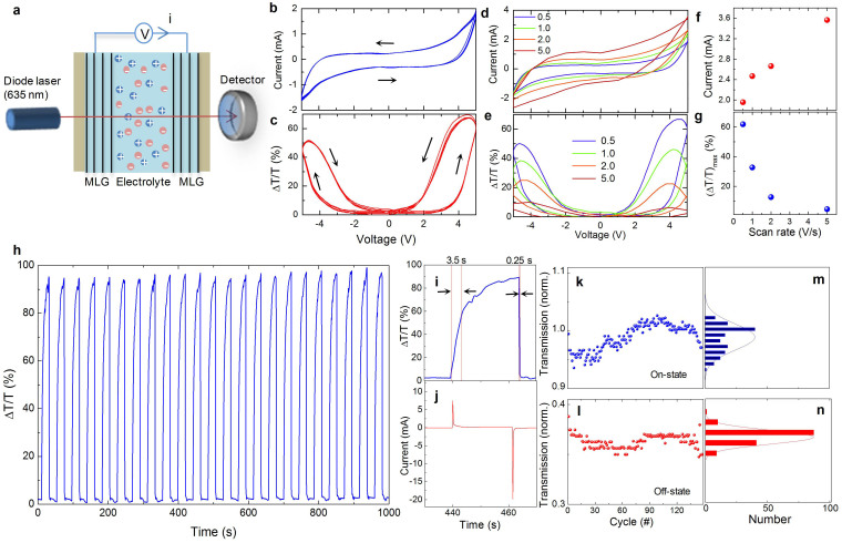
Figure 4. Charging and discharging characteristics of graphene electrochromic devices.
(a), Schematic illustration of the experimental setup used for the simultaneous electrical and optical characterization of the graphene electrochromic devices. (b), Current-voltage and (c), transmittance-voltage curves at 635 nm at a scan rate of 0.5 V/s. (d), Current-voltage and (e), transmittance-voltage for different scan rates. (f), Maximum current and (g), maximum optical modulation versus the scan rate. (h), Optical switching characteristics of the device at 635 nm. (i,j) Time variation of transmittance and charging current for a single switching cycle. The extracted RC time constants of the electrochromic device (3.5 seconds for charging and 0.25 seconds for discharging respectively) are illustrated on the single switching cycle with intervals defined by the red bars. (k,l), Long term stability of the transmittance in the on-state (at 5 V) and off-state (0 V). (m,n), The histogram of the transmittance in the on- and off-state.

