
Figure 1.
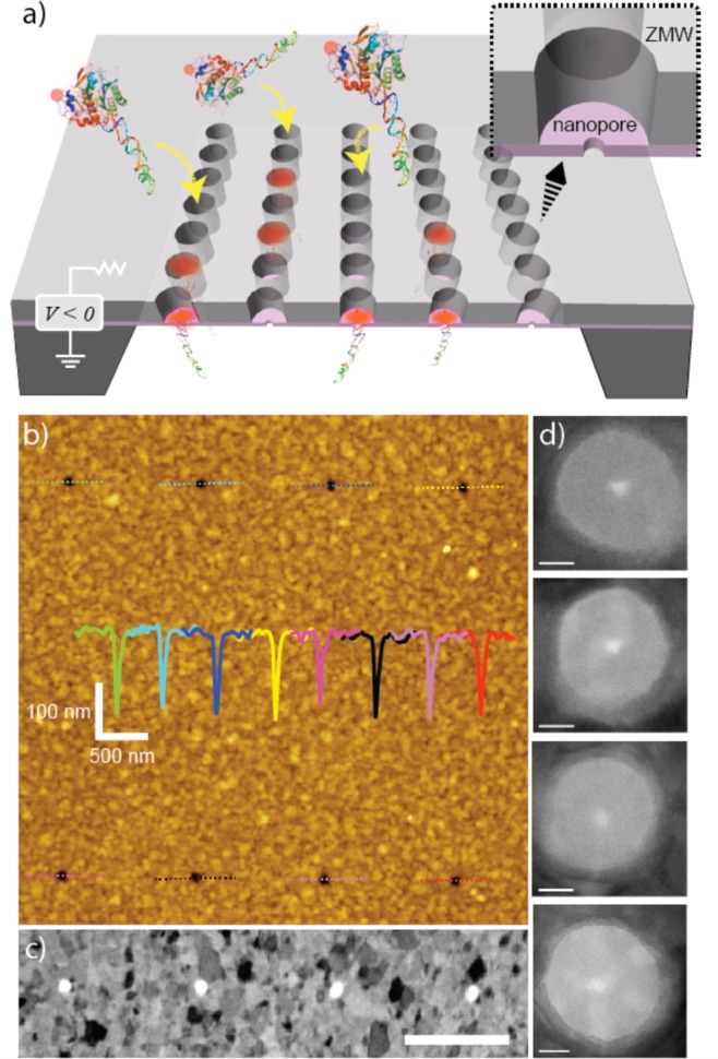
NZMW device. (a) Scheme of the NZMW. An array of ZMWs is positioned on a 35 nm silicon nitride membrane with nanopores at the bases of waveguides (inset). A voltage bias actively draws complexes of biotinylated DNA and fluorescently labeled streptavidin to the pore, which places the fluorophore in the ZMW excitation volume. (b) An AFM scan of the ZMW membrane illustrates the topography of the surface. ZMWs are spaced 1.3 μm × 4 μm. Line scans of each ZMW demonstrate uniformity with an average top diameter of 86.2 ± 6.4 nm (N = 21). The scans have a pointed bottom profile because the AFM tip cannot penetrate the full depth of the waveguide. (c) Dark-field scanning transmission electron micrograph (inverted contrast) of four ZMWs in the array (scale bar = 1 μm). (d) TEM images of ZMWs with 3 to 3.5 nm nanopores drilled in their centers (scale bars = 20 nm). ZMWs have a measured base diameter of 64.9 ± 3.7 nm (N = 57).