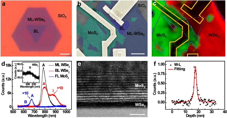
Figure 2.
Structural characterization of the WSe2/MoS2 heterojunction p–n diode. (a) Optical microscopy image of a truncated triangular domain of monolayer WSe2 with an inverted triangular bilayer region at the center. (b) The false color SEM image of the WSe2/MoS2 vertical heterojunction device, with ML-WSe2 highlighted by blue color, BL-WSe2 area by violet color, MoS2 by green color, and metal electrodes by golden color. The scale bar is 3 μm. (c) The PL mapping of the WSe2/MoS2 heterojunction device, with red color representing the PL from MoS2 and the green color representing PL from WSe2. (d) The PL spectra of synthetic ML- and BL-WSe2 and few-layer MoS2 flakes with the A, B exciton peaks and indirect transition I peak labeled. The intensities of BL-WSe2 and FL-MoS2 are multiplied by 10 times for better visibility. Inset, the B exciton peak in ML- WSe2. (e) The cross-sectional HRTEM image of the WSe2/MoS2 heterojunction interface. The scale bar is 5 nm. (f) The EDS element distribution profile from the bottom to the top of panel e. The black square represent the distribution profile of W-L characteristic peaks. The red line represents the fitting curve for W-L distribution profile, with a full width at half-maximum of 1.2 nm, corresponding to bilayer WSe2.

