Figure 3.
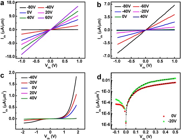
Electrical characterization of the WSe2/MoS2 heterojunction p–n diode. (a) The Ids–Vds characteristics of n-type MoS2 FET transistor with Ni/Au (5/50 nm) contacts. (b) The Ids–Vds characteristics of p-type WSe2 FET transistor with Au (50 nm) contacts. (c) Gate-tunable output characteristics of the WSe2/MoS2 heterojunction p–n diode. (d) The derivation of the p–n diode ideality factor by using a model consists of an ideal p–n diode with a series resistor. An ideality factor of 1.2 was derived with a series resistor of 80 MΩ at 0 V gate voltage (red circle), and an ideality factor of 1.3 was derived with a series resistor of 33 MΩ at −20 V gate voltage (green triangle).

